
Rabbit Radar Overview
“The NCSU Rabbit Radar”
Matthew Dwyer () and David S. Ricketts ()
North Carolina State University. Raleigh, North Carolina, United States of America.
We present the design and hand fabrication of a frequency modulated continuous wave (FMCW) radar that teaches practicing engineers and students the fundamentals of radar theory, microwave systems and component design. The fabrication can be done by hand cutting simple shapes of foil with a knife or by cutting more complex shapes of foil with a 2-D cutter from a hoppy store [1]. We present a brief overview of the theory of operation for the FMCW system and each component used. Then the design procedure for each component is presented along with experimental results from the fabricated components. The frequency of operation was chosen to be 925 MHz, or around 1 GHz. This decision was made for multiple reasons. First, the frequency is within an ISM band. Second, this enabled easy fabrication of microwave transmission line circuits (/4 is roughly 40 mm) and as well as hand soldering of discrete components for termination and amplifier biasing. Operation at 2.4 GHz ISM band for non-North American applications is a simple shift of frequency in the design targets, but the theory remains the same.
The goal is to have a FMCW Radar which can be designed and built in one day by a group of four to five professional or graduate student engineers. This FMCW Radar will be highlighted at RFIC2020 and IMS2020 as a dedicated practical session for attendees to build a FMCW Radar while attending either conference. This work is, in part, builds upon the authors Bits2Waves radio workshop and course [1] and is in part, inspired by the “Coffee Can Radar” [9]..
FMCW Theory
The FMCW Radar is a simple radar that can measure the distance of a static object and the velocity of a moving object. The basic principle of any Radar is to emit an electromagnetic signal and measure its reflection from a target, Fig. 1(a). The reflection occurs due to the metallic surface of the target that scatters energy in all directions, a small amount of which the Radar receives. The simplest Radar would be to emit a continuous wave and measure the reflected, or scattered, signal. The problem is that the received signal would have the same frequency as the transmitted signal, with only a phase difference. This would result in only being able to estimate the distance as
![]() (Eq. 1),
(Eq. 1),
where d is the estimated distance, n is any integer value, is the wavelength and is the phase difference between the transmitted and received signals. As one can see, the distance is ambiguous, as the distance could be any integer multiple, n, of the wavelength. In addition, such a system would be sensitive to multi-path as well as phase delays in the transmit and receive hardware. The velocity of a moving target, however, could be measured by this simple radar due to the doppler shift, where the frequency difference is directly related to the velocity of the object:
 (Eq. 2),
where fo is the transmit frequency, v is the velocity of the object and c is the speed of light.
 |
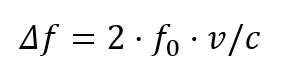
| Figure 1: (a) System architecture of the FMCW Radar. (b) Frequency sweep and delay time roundtrip to target creates a t that is measured as a f. (c) Mixer. (d) Coupler. (e) PA and LNA. (f) Antenna. |
A solution to the distance ambiguity problem is to use a frequency swept Radar, such as a FMCW Radar [2]. As shown in Fig. 1(b), the frequency to the transmitter is swept between a start and stop frequency in a linear fashion. The target distance (d) will result in a reflected signal that is delayed by t, where t is the sum of the travel time of the outgoing transmit signal, which is sent from the Radar to the target, and the return time of the transmit signal, which is reflected from the target back to the Radar. Due to this time difference, the received signal will be shifted in time. When the signal returns to the receiver, it will be at a different frequency than the transmit frequency since the VCO has changed frequencies during t . This change in frequency can then be used to determine the absolute distance without ambiguity. The distance is
![]() (Eq. 3)
(Eq. 3)
Where
![]() (Eq. 4)
(Eq. 4)
and m is the slope of the frequency ramp in Hz/s, Fig. 1(b). Measuring a change in frequency can easily be done with a simple homodyne radio [2,3].
Figure 1(a) shows the basic system design of a FMCW Radar. A voltage-controlled oscillator (VCO) is swept between two frequencies by a linear ramp. The voltage-frequency transfer function of the VCO along with the control signal ramp will determine the slope, m. The voltage-frequency transfer function of a VCO is typically non-linear; therefore, a linear control signal will not result in a linear frequency sweep. For first order designs this can be ignored. For higher performance designs, a phase-locked-loop can be used to ensure a linear control signal results in a linear frequency sweep. An example part to accomplish this is the Analog Devices ADF4158.
The VCO output signal is fed to a power amplifier (PA), Fig. 1(e), where the signal is amplified. The PA output signal is then split by a splitter into a power signal and a local oscillator (LO) signal. The splitter in this design is an edge-coupled microstrip coupler with approximately -15 dB coupling, shown in Fig. 1(d), such that the LO is 15 dB below the power signal. The power signal is fed to a wide-bandwidth antenna. For this design, we chose an antipodal Vivaldi antenna, which is easy to build and has a wide bandwidth, Fig. 1(f) [4]. The receiver is a second antenna that feeds a low-noise amplifier (LNA), shown in Fig. 1(e). The output of the LNA is then down converted by a branchline mixer, shown in Fig. 1(c). using the LO signal produced by the splitterThe down converted signal from the branchline mixer is then filtered and amplified to be measured. To allow ease of access for designers and builders, we down convert the received signal to the audio frequency range (20 Hz to 20kHz) so that the ADC in a laptop microphone port can record it. An MP3 recorder, such as in your phone, would work just as well. We can then read in the digitized frequency data from the MP3 file and plot it to see the distance of any target. Velocity can easily be measured through the change in distance over time (for low velocities). Higher velocities will cause significant Doppler shifts and thus an error in the Radar. This is not covered in this short article and workshop.
Power and Low-Noise Amplifier Design
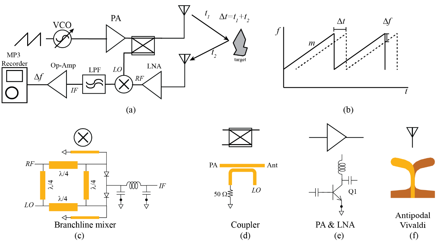
The schematic of the amplifier bias is shown in Fig 2(a). We use the same transistor, the BFU550, for the PA and LNA to simplify construction. The difference between the two designs will be the bias condition and the input and output matching network impedances. The gray portion of the bias network is the DC bias. R2 sets the base current for Q1. R1 and C3 form a simple feedback circuit that helps regulate the operating voltage on C3. The input voltage, approximately 9V from a 9V battery, is reduced by the voltage drop in R1. As the collector current increases (DC), this drop will increase, reducing the voltage on the bias resistor R2, causing the bias to reduce and with it a rduction in collector collector current. This feedback network is not critical to the biasing; however, it assists in bias regulation. The RF path is through Q1, to the output load (C1 and C2 are simple DC blocking capacitors). The amplifiers run in Class-A (linear) and Class-AB (non-linear) depending on the input signal. Small signals will be Class-A [5].
 |
| Figure 2: (a) Schematic of PA and LNA. R1 is 75k for LNA and 10k for PA. (b) Load pull results showing ideal load impedance. Also shown is the input impedance for that load impedance. (c) Gain and NF circles for LNA. The source impedance is a tradeoff between noise and gain. The load impedance is set for maximum gain. (d) & (e) Simulation vs. measured results for the LNA and PA. |
The PA is designed by optimizing the output impedance, through L3 and L4, to maximize output power. The transistor is biased at 30 mA DC current, which is near the maximum output power on the transistor data sheet. To design the PA, we perform a Load-Pull analysis, where we sweep the output impedance in simulation over a range of the Smith Chart. We then measure the output power and find the load impedance with the highest output power. Figure 1(b) shows the load-pull results. The black crosses are the load impedance simulated, and the circles are of constant output power (blue) and power added efficiency (PAE) (red). We selected a load impedance of 50+58j which was near the maximum power point (center most circle in blue). We impedance transform a 50 load to this target impedance in our PA so that it sees the optimal load impedance for maximum output power. The input impedance matching network is assumed to operate in the small signal range, so we simply look for an impedance matching network that will impedance match the 50 input cable to the input of the PA. The PA input is 40-22j , Fig. 2(b) which means our network should transform 50 to 40+22j , i.e. the complex conjugate to ensure impedance matching. It is important to note that for the PA load, we swept the actual loads we wanted, so there is no complex conjugation. In fact, one typically does not think of “matching” the PA output with a network, but rather finding the load that produces the maximum power [6]. This is because most PAs operate in non-linear regime where small signal matching does not apply (or is not the best approach).
The LNA is biased at 3 mA, which is closer to the lower noise operation of the transistor as shown in the datasheet. The amplifier is then simulated to find the output impedance that achieves the maximum gain (Gmax). This was found, Fig. 2(c), to be 60+100j . Note that the maximum gain circles (blue) extend off of the Smith Chart. We chose a point on the highest circle, but closest to the origin, i.e. closest to 50 , in order to minimize the impedance transformation needed. The source network is where the LNA differs from a simple ac amplifier. The input referred noise of the amplifier is dependent on the impedance seen at the input. As a result, an impedance matched input may not provide the lowest noise operation. Many transistors have been measured and modeled for the source impedance that yields the lowest noise – measured by the noise figure (NF). The noise factor, F, is the ratio of the signal to noise ratio of the input to the signal to noise ratio of the output, NF is 10log10F. Noise figure (NF) is always greater than zero. Figure 2(c) shows the gain circles for input impedance that achieves maximum gain (green), it assumes the load is the load that achieves maximum gain, i.e. 60+100j. Plotted in brown are the source impedances for minimum NF. Note the two overlap but are not identical. We selected a source impedance of 11+10j as a compromise between high-gain and minimal noise.
For all impedance matching networks, a simple two transmission line (t-line) network was chosen, which consists of a series t-line with an open t-line stub, Fig. 2(a). While one can calculate the lengths of each t-line [L1 through L4 Fig. 2(a)], most commercial simulation tools can “tune” component parameters. The characteristic impedance of the t-lines was fixed at 50 for ease of fabrication; only the lengths were modified. Our Radar was designed in National Instruments AWR Microwave Office, which allowed us to tune the lengths on a slider. In less than a minute one can adjust the lengths by trial and error to get the desired impedances. An optimization feature in the software can also find suitable values. The network is then attached to a 50 t-line to extend the network to the edge of the board in order to connect a PCB mount SMA connector.
Figure 2(c) show the S-parameter results of the PA and LNA. The general performance is good, however there are discrepancies from simulations. These discrepancies result from the impedance matching networks not being accurate due to a lack of consideration of the board edges and variations in fabrication using a simple 2-D foil cutter.
Branchline Mixer
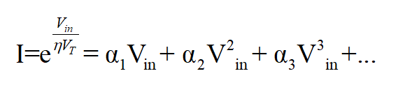
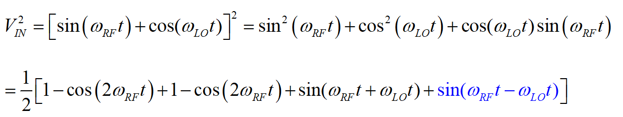
The Branchline mixer is an RF down converting mixer that does not require any transformer or balun. The mixer is composed of three parts: 1) a branchline coupler to create a quadrature component of each input signal, the RF and LO, and to combine those two signals; 2) A diode with a nonlinear voltage to current transfer function (as all diodes have); and, 3) a low pass filter (LPF) to remove the RF and LO and leave only the intermediate frequency (IF). The branchline coupler, Fig. 3(a), splits the signals at the RF and LO ports into two signals with 90 degrees of phase shift. The RF is split into the two output ports, creating a sine and cosine version of the RF. Likewise, the LO is split into the two output ports and creates a sine and cosine version of the LO. Thus, at the terminals of each diode, there is a signal which is sin(RFt)+cos(LOt) or sin(LOt)+cos(RFt). A virtual ground exists at the junction of the two diodes. In each diode, the voltage to current transfer function is an exponential, which can be approximated by a Taylor series:
 Eq. 5
Eq. 5
The mixer uses the square term to provide the “mixing” or multiplication. The square term will produce
 Eq. 6
Eq. 6
The last term (in blue) is our desired term. Note that all other powers of Vin in Eq. 5 will produce additional harmonics. The job of the mixer is to filter or cancel as many of these other unwanted harmonics as possible. From the first term, Vin will produce LO and RF signals in the diode and since 1 is typically the largest coefficient in a Taylor series, their contribution to the output signal will be significant. While a down converting mixer could filter them out, we can also cancel them by adding the current from two diodes whose voltages are opposite. The opposing polarity of the two diodes in the branchline mixer achieves this. Figure 3(c) shows the diode currents for a single and dual diode configuration. One can see that the dual diode significantly cancels the LO.
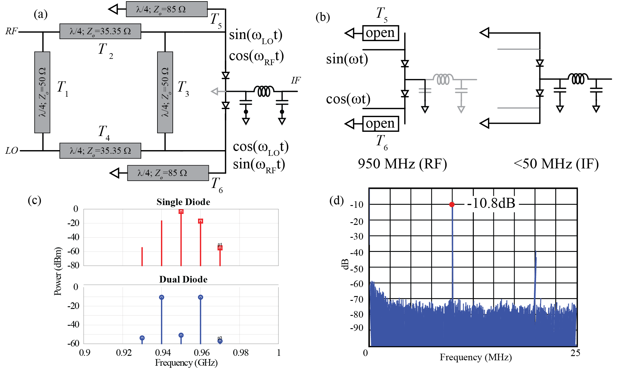 |
| Figure 3: (a) Branchline mixer. The branchline consists of four /4 sections, with the top and bottom at 35 and the left and right at 50 [2]. The Branchline separates each input into two outputs with a 90-degree phase shift. Two /4 sections are added to provide a DC path to ground for the mixer, but are open at RF. (b) Shows operation at RF and IF frequencies, where black indicates the active components/paths. (c) Current in a single diode and a balanced, 2-diode, mixer, where the LO at 950 MHz is cancelled. (d) Measured results of mixer showing a -10.8 dB of conversion loss (simulated was -7.3 dB). |
The remaining harmonics are removed by the low-pass filter at the output. To ensure proper operation of the diodes, a DC path to ground is provided through two /4 transmission lines, T5,6 connected from ground to the output of the branchline. T5,6 will impedance transform the ground to an open at RF and LO frequencies. At DC the L5,6 will simply be a short to ground. Thus, T5,6 do not play a role at RF. The DC and RF operation is shown in Fig. 3(b), where the open at RF and short at DC are shown. The junction of the two diodes should be a short at RF frequencies. This could be done by a /4 transmission line with an open end (transforming an open to a short at RF and LO frequencies), however electromagnetic simulations show that owing to the low dielectric constant of FR4, the /4 transmission line with an open termination acts more as an antenna and becomes a major source of loss. To overcome this, and to ease fabrication, we chose a discrete LC -filter, with capacitors in the shunt legs. These capacitors serve as the ac short for the diodes and do not suffer from any radiation problems. The down converted signal is shown in Fig. 3(d). The simulated conversion loss was -7.26 dB and the measured conversion loss was -10.8 dB.
Coupler
In the Radar design an LO signal matching the transmit frequency is needed. This can be done by splitting the VCO prior to the PA with a splitter, such as a Wilkinson divider [2]. Another option is using a directional coupler, which can be placed after the PA and has a coupling ratio designed such that it provides 0 to 2 dBm of LO power. In this design, we opted for the directional coupler, as it is an interesting device to design and build for the microwave designer.
The directional coupler consists of two edge-coupled transmission lines, Fig. 4(a) and (b) with four ports, P1 through P4. The coupling occurs from the overlap of fields between the two microstrip conductors. The analysis of the coupler uses a basic analysis approach in microwave design – splitting the input signal into even and odd modes and analyzing each one independently. Figure 4(a) shows how a single ended input can be split up into an even mode (in phase, same potential) and an odd mode (opposite phase, opposite potential). We will see shortly that the analysis for even and odd modes can be simplified due to symmetry.
Figure 4(b) shows two modes that exist when two microstrip t-lines are placed in parallel. The first is an even mode, where the voltage on the two t-lines is the same. In this case, there is no difference between the potentials of the transmission lines and any coupling capacitance which may exist will see a constant voltage and thus does not have an effect. The impedance of each line is determined merely by the fields from the microstrip to the ground plane, which is shown by C11,22; we assume the inductance per unit length is the same for all modes. The second mode is the odd mode, where the signals have opposite phase (and potential) on each t-line. In this instance, the potential between the two lines changes with time and therefore the coupling capacitance has an effect. The characteristic impedance of the odd mode is now dependent of both C11,22 and C21. It is worth emphasizing that the difference in characteristic impedance for the even and odd modes are due to the coupling capacitance. Thus, the differing impedance is a result of the coupling; and analyzing the differing impedance is directly related to the coupling.
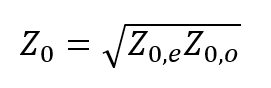
To find the coupling between two microstrip t-lines, we apply a signal to Port 1 (P1) and see the level of signal that appears on Port 3 (P3), which is used as our LO port in Fig. 1. The voltage, V1, is determined by the voltage divider between the source impedance, Z0, and the input impedance of the t-line, ZIN. ZIN can be found using the standard relationship for terminated t-lines [2]:
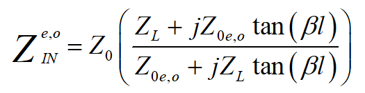 Eq. 7
Eq. 7
where ZL is the load impedance [Z0 in this Fig. 4(a)], l is the length of the t-line and is the propagation constant. Z0e,o is the characteristic impedance for the even and odd mode. One can see, that the difference in Z0e,o will result in different ZIN.
The voltages, V1 and V3, may be calculated for each mode as follows:
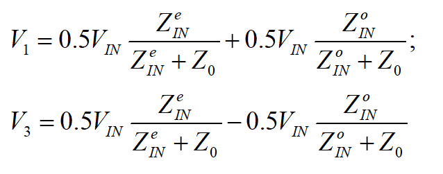 Eq. 8 and Eq. 9
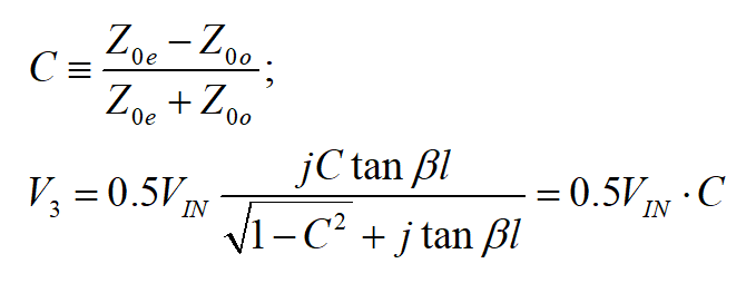
If the impedances were the same for each mode and equal to the characteristic impedance of the source (VIN), then V1=0.5VIN and V3=0. However, due to the mutual coupling, the even and odd impedances are not the same. As a result, there will be a voltage, V3, on Port 3, P3. By making the assumption that
 (Eq. 10)
and that the t-lines are a quarter wavelength, we can write the voltage on V3 as [7]:
 Eq. 11 and 12
where we used l=π/2 for a quarter wavelength. With this, we can then calculate the fraction of the input that appears on P3 from the difference in the characteristic impedances of the even an odd mode. We can calculate the even and odd mode impedances needed from the desired coupling factor, C. Not derived here but worth mentioning, P4 will be isolated with no signal and P2 will have a slight reduction in voltage, as would be expected due to energy flowing out of P3.
 |
| Figure 4: (a) Even/odd mode analysis of coupled lines. (b) Cross section of coupled microstrip lines. (c) Layout of coupler. (d) Simulation and measured results of coupler. |
To design the coupler, we need to design the coupled lines for the proper even and odd mode impedances. Techniques to do this without simulation have been reported [7], but from a practical perspective, the only two design variables are the width of the t-lines and the spacing between them, S. For our design we choose the same width as our standard 50 lines, 2.8mm, and thus the only design variable is the spacing. Using NI AWR Microwave Office, we are able to tune the spacing and see the change in coupling. It is very simple to set the value of S such the coupling is the desired -15 dB, which is S=1 mm spacing for our microstrip lines. Fig. 4(d) shows the simulated vs. measured results of the coupler. We obtained -17 dB coupling and good reflection and isolation.
Antipodal Vivaldi Antenna
For a FMCW Radar, a broadband antenna is typically needed. In the example presented here, the bandwidth is only 3%, which could be achieved by several antenna designs. From a practical perspective, the handmade antennas result in a significant variation in antenna center frequency. We have found that the tapered slot [4], or Vivaldi, antenna is an attractive choice, owing to its simplicity to hand-fabricate and very broad bandwidth, which relaxes the need for precise center frequencies. In our design we adopt an antipodal version that will take a microstrip input and transition it to a balanced, tapered slot. Fig. 5 shows the antenna which has been referred by some as a “rabbit ear” antenna, due to the shape of the conductors. It consists of two conductors on either side of a 3.175 mm thick rigid plastic board, commonly used for yard signs, Fig. 5(a). The plastic board is filled with air and thus has a relative dielectric constant of 1. The antenna consists of three parts: 1) a 50 microstrip input, 2) a tapered transition to a parallel trace waveguide and 3) a tapered slot antenna. The fields at the input are between the microstrip and the ground plane of the opposing conductor. As the signal moves outward it slowly transitions to a differential signal between the conductors at the tapered slot.
The design criteria are quite relaxed. The length of Sections 1 and 2 in Fig. 5(a) should be enough to make the transition of the fields smooth. The tapering of the slot line needs only to be a relatively smooth contour, although many papers have attempted to find a mathematically optimal shape, such as a square law shaped design, an exponential shaped design and a simple circular shaped design. The only parameter of relevance is the final width of the taper, which would be a half-wavelength at the largest part. For our design, a 50 microstrip input using the relative dielectric constant of air is 15 mm wide, which sets the initial trace width. Using the target frequency of 925 MHz, the final width is set at approximately 15 cm. The total length is between 1.5 and 2 times the width. The rounded corners of the end assist in making a smooth frequency transition at the lower frequency band.
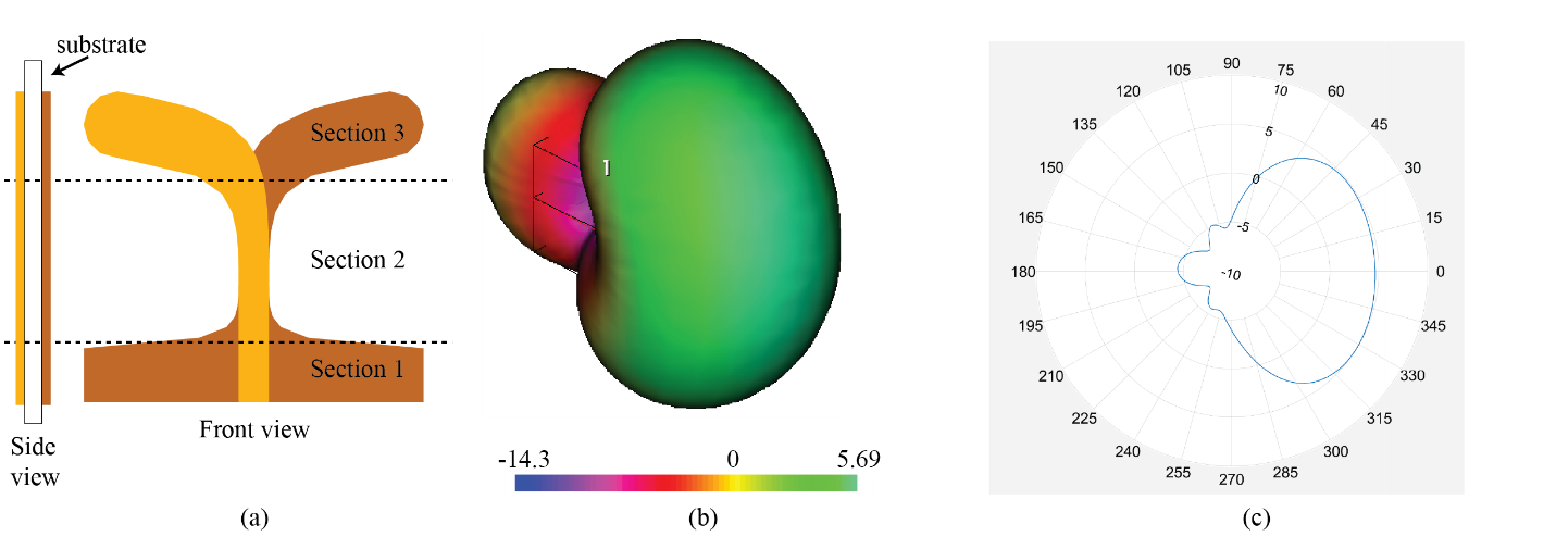 |
| Figure 5: (a) Antipodal Vivaldi antenna. Note the different colors represent the top and bottom layers. The three sections of the antenna are marked. (b) Simulated radiation pattern with a peak gain of 5.69 dBi. (c) Polar plot of the measured radiation pattern. The gain is just above 5dBi. |
Most antipodal antennas rely on some parameter sweep to optimize their design. In our Radar, we took advantage of NI’s AntSym software, which uses a genetic algorithm to optimize antenna design. We chose only the bandwidth, outline dimensions, and targeted gain (7 dB) and the software optimized the shape. The output design was then imported in to the AWR Axiem software and a full EM simulation was done, which also allowed S-parameter measurements and integration with radio components for simulation. The simulated radiation pattern is shown in Fig. 5(b). The measured antenna pattern is shown in Fig. 5(c). The antenna achieves greater than 10% bandwidth (which is quite small for this type of antenna) and good gain of greater than 5 dBi.
VCO and Control
For the Radar design, we used a commercial VCO, the ZX95-1012-S+ from Mini-Circuits. This VCO has a 0 to 5V tuning range. The control signal can be generated by a simple function generator. We built a hobby function generator based on the XR2206 IC [8]. The output of the VCO was 0 dBm and the frequency swept was approximately 30 kHz (this small sweep was chosen to keep the IF frequency in the audio spectrum for easy measurement by a laptop or MP3 recorder).
IF Amplification and Filtering
The output of the mixer has already been filtered by the mixer; however, the amplitude is still too low for a standard audio recorder. Two second order low-pass filters were built using an OPA1679 quad op-amp, show in Figure 6. A variable gain op-amp amplifier was placed at the input along with an ac coupling capacitor. The gain for each stage was 10 V/V and with the adjustable input amplifier the gain could be varied between 10 V/V and 1000 V/V. The filters were set to 20 kHz bandwidth according to the following equation:
Eq. 13
 |
| Figure 6: The schematic for the IF amplifier. The first stage is an ac coupler and variable gain through RA1. The second two stages amplify the signal and provide two second order filters, all with fc=20 kHz. |
Final System Test
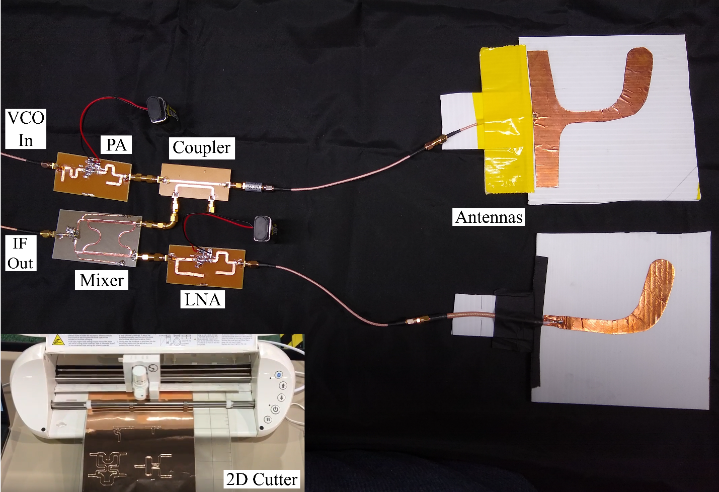
The radio was assembled as shown in Fig. 1. An image of the connected radio is shown in Fig. 7(a). The individual components can be seen, including the PA, LNA, coupler and mixer. The impedance matching networks of the PA and LNA are clearly seen as the meandered t-lines at the input and output ports. The assembly of the components was done by hand using a 2-D cutter (Silhouette Portrait 2 Electric Cutting Tool) and standard tools. Details on component fabrication methods can be found on the From Bits to Waves website [1].
 |
| (a) |
 |
| (b) |
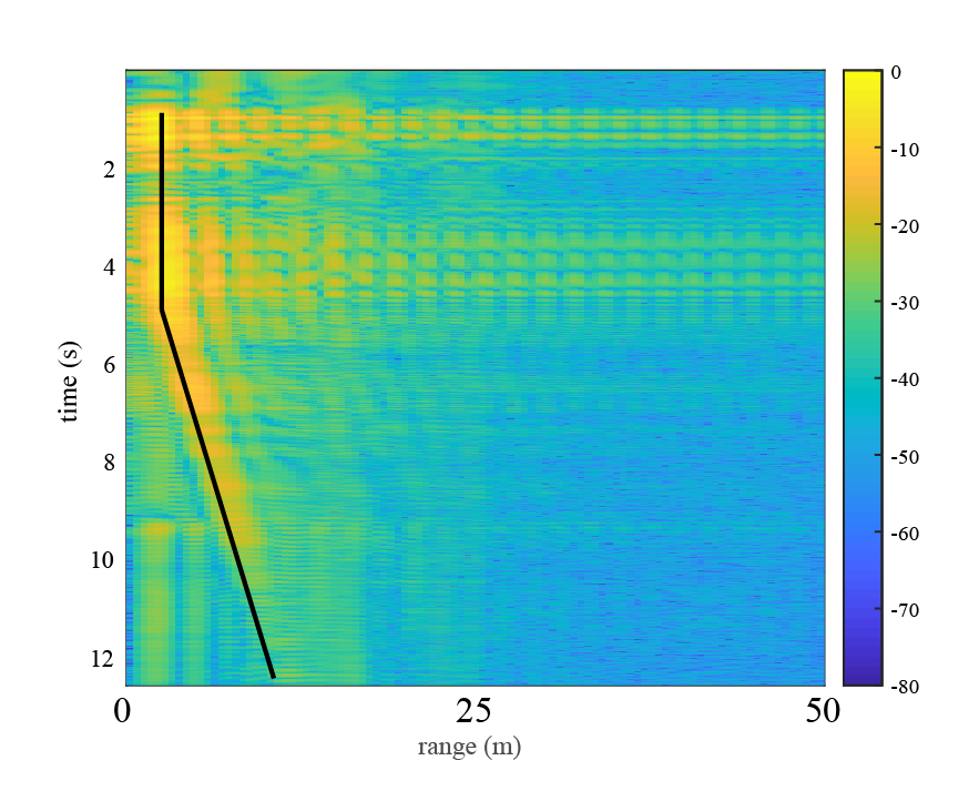
| Figure 7: (a) photograph of radio system (Photograph by Matthew Dwyer). (b) measurement results of person standing in front of radar and then moving quickly away. The black line is added to highlight the trajectory. |
The radio was tested by having a target of 0.25 m2 aluminum foil covered board placed in front of the radar. To illustrate the receive signal, the target was moved during measurement so that the change in reflected signal can clearly be seen. Fig. 7(b) shows the change in distance over time, demonstrating the functioning radar. The plot was scaled using the slope of the frequency versus the time of the oscillator. The audio signal was recorded using Audacity on a PC laptop and the plot made in MATLAB. The MATLAB code is based on a similar radar project [9]. A synchronous signal from the sweep generator is needed for the software to know when a new sweep is initiated. We used a trigger signal from our voltage sweep generator on a stereo input to the PC. One channel recorded the received signal and the other the synchronizing trigger. The MATLAB code parsed the received signal into individual section and analyzed the frequency difference. The code from [9] was leveraged for this function.
The resulting plot is simply a waterfall plot, where the x-axis is the f received, which has been scaled to give distance in meters (which are linearly related to one another). The y-axis is simply measurement time, with each new line representing a different time sweep, thus the data “falls” from line to line as time increases. Note the start time is the top line.
Conclusions
This article presented a FMCW radar build from basic microwave components that were constructed by hand from off the shelf discrete components and cut copper foil. The operation of the radar was demonstrated in static and dynamic reception with a proud graduate student walking backward with a target. Since the antennas of this radar resemble rabbit ears, this might be coined the “NCSU Rabbit Radar” in similar fashion to the “MIT Coffee Can Radar” [9,10].
Acknowledgements
The authors would like to thank Prof. Michael Steer for his guidance and support, Ms. Sherry Hess from NI AWR for her support of the design development, Mr. Mark Saffian of NI AWR for is tireless help in sorting out design details and Dr. Junyu Shen who assisted with measurements and early development of the circuits used. We would also like to acknowledge the inspiration of the “Coffee Can Radar” which built a FMCW radar using commercial off the shelf parts (COTS) [9,10]. We utilized their MATLAB scripts and system design in our work here.
References
[1] D. S. Ricketts, “Bits2Waves – Build a 16 QAM 950 MHz Radio,”. [Online].
Available: http://www.rickettslab.org/bits2waves/fabrication. [Accessed Jul. 1, 2019].
[2] Michael Steer, Microwave and RF Design, Scitech Publishing, 2013.
[3] Steven. W. Ellingson, Radio Systems Engineering, Cambridge Press, 2016.
[4] Ultra-Wideband Antennas and Propagation: For Communications, Radar and Imaging
Ben Allen (Editor), Mischa Dohler (Editor), Ernest Okon (Editor), Wasim Malik (Editor), Anthony Brown (Editor), David Edwards (Editor), John Wiley & Sons, 2007. ISBN: 978-0-470-03255-8
[5] Guillermo Gonzalez, Microwave Transistor Amplifiers, Prentice Hall, 1997.
[6] Steve Cripps, RF Power Amplifiers for Wireless Communications, Artech House Microwave Library.
[7 David M. Pozar, Microwave and RF Design of Wireless Systems, John Wiley & Sons, Inc. 2001.
[8] Online: Signal Generator DIY Kit, KKmoon XR2206 High Precision Function Signal Generator DIY Kit Sine/Triangle/Square Output 1Hz-1MHz Adjustable Frequency
[9] Gregory Charvat, Jonathan Williams, Alan Fenn, Steve Kogon, and Jeffrey Herd. RES.LL-003 Build a Small Radar System Capable of Sensing Range, Doppler, and Synthetic Aperture Radar Imaging. January IAP 2011. Massachusetts Institute of Technology: MIT OpenCourseWare, https://ocw.mit.edu. License: Creative Commons BY-NC-SA.
[10] MIT radar course”: K. E. Kolodziej et al., “Build-a-Radar Self-Paced Massive Open Online Course (MOOC),” 2019 IEEE Radar Conference (RadarConf), Boston, MA, USA, 2019, pp. 1-5.