
Directional Coupler
Directional Coupler
The directional coupler is used to split the power from the output of the power amplifier to be used as the local oscillator (LO) of the branchline mixer. We want to split the power as we need the branchline mixer to compare the frequency of the output of the PA to the received frequency. If the power amplifier (PA) has 10-15 dB of output power, a split of -15dB is a good target for design.
Theory
In the Radar design an LO signal matching the transmit frequency is needed. This can be done by splitting the VCO prior to the PA with a splitter, such as a Wilkinson divider [2]. Another option is using a directional coupler, which can be placed after the PA and has a coupling ratio designed such that it provides 0 to 2 dBm of LO power. In this design, we opted for the directional coupler, as it is an interesting device to design and build for the microwave designer.
The directional coupler consists of two edge-coupled transmission lines, Fig. 4(a) and (b) with four ports, P1 through P4. The coupling occurs from the overlap of fields between the two microstrip conductors. The analysis of the coupler uses a basic analysis approach in microwave design – splitting the input signal into even and odd modes and analyzing each one independently. Figure 4(a) shows how a single ended input can be split up into an even mode (in phase, same potential) and an odd mode (opposite phase, opposite potential). We will see shortly that the analysis for even and odd modes can be simplified due to symmetry.
Figure 4(b) shows two modes that exist when two microstrip t-lines are placed in parallel. The first is an even mode, where the voltage on the two t-lines is the same. In this case, there is no difference between the potentials of the transmission lines and any coupling capacitance which may exist will see a constant voltage and thus does not have an effect. The impedance of each line is determined merely by the fields from the microstrip to the ground plane, which is shown by C11,22; we assume the inductance per unit length is the same for all modes. The second mode is the odd mode, where the signals have opposite phase (and potential) on each t-line. In this instance, the potential between the two lines changes with time and therefore the coupling capacitance has an effect. The characteristic impedance of the odd mode is now dependent of both C11,22 and C21. It is worth emphasizing that the difference in characteristic impedance for the even and odd modes are due to the coupling capacitance. Thus, the differing impedance is a result of the coupling; and analyzing the differing impedance is directly related to the coupling.
To find the coupling between two microstrip t-lines, we apply a signal to Port 1 (P1) and see the level of signal that appears on Port 3 (P3), which is used as our LO port in Fig. 1. The voltage, V1, is determined by the voltage divider between the source impedance, Z0, and the input impedance of the t-line, ZIN. ZIN can be found using the standard relationship for terminated t-lines [2]:
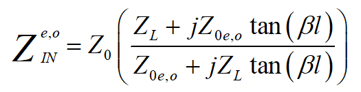 Eq. 7
Eq. 7
where ZL is the load impedance [Z0 in this Fig. 4(a)], l is the length of the t-line and is the propagation constant. Z0e,o is the characteristic impedance for the even and odd mode. One can see, that the difference in Z0e,o will result in different ZIN.
The voltages, V1 and V3, may be calculated for each mode as follows:
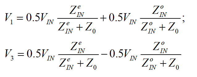 Eq. 8 and Eq. 9
If the impedances were the same for each mode and equal to the characteristic impedance of the source (VIN), then V1=0.5VIN and V3=0. However, due to the mutual coupling, the even and odd impedances are not the same. As a result, there will be a voltage, V3, on Port 3, P3. By making the assumption that
 (Eq. 10)
and that the t-lines are a quarter wavelength, we can write the voltage on V3 as [7]:
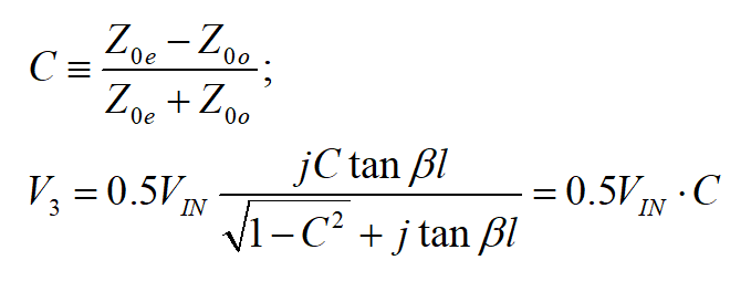 Eq. 11 and 12
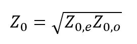
where we used l=π/2 for a quarter wavelength. With this, we can then calculate the fraction of the input that appears on P3 from the difference in the characteristic impedances of the even an odd mode. We can calculate the even and odd mode impedances needed from the desired coupling factor, C. Not derived here but worth mentioning, P4 will be isolated with no signal and P2 will have a slight reduction in voltage, as would be expected due to energy flowing out of P3.
 |
| Figure 4: (a) Even/odd mode analysis of coupled lines. (b) Cross section of coupled microstrip lines. (c) Layout of coupler. (d) Simulation and measured results of coupler. |
To design the coupler, we need to design the coupled lines for the proper even and odd mode impedances. Techniques to do this without simulation have been reported [7], but from a practical perspective, the only two design variables are the width of the t-lines and the spacing between them, S. For our design we choose the same width as our standard 50 lines, 2.8mm, and thus the only design variable is the spacing. Using NI AWR Microwave Office, we are able to tune the spacing and see the change in coupling. It is very simple to set the value of S such the coupling is the desired -15 dB, which is S=1 mm spacing for our microstrip lines. Fig. 4(d) shows the simulated vs. measured results of the coupler. We obtained -17 dB coupling and good reflection and isolation.
Below is a video explaining the theory of the directional coupler. Note, it is from a longer video, but starts at the point of the directional coupler.
Please start it at 1:00:17 for the directional coupler.
Design
To design transmission lines for this workshop, you will need to use TXLINE, which is included in AWR under Tools->TXline
You may also find it here in the template files for the workshop.
Determine the Width and Length of the transmission lines using TXLINE. TXLINE can be found under Tools-TXLINE. It is a calculator to help you convert electrical parameters such as electrical length and impedance to a physical implementation. The following screen shot show the calculator interface.
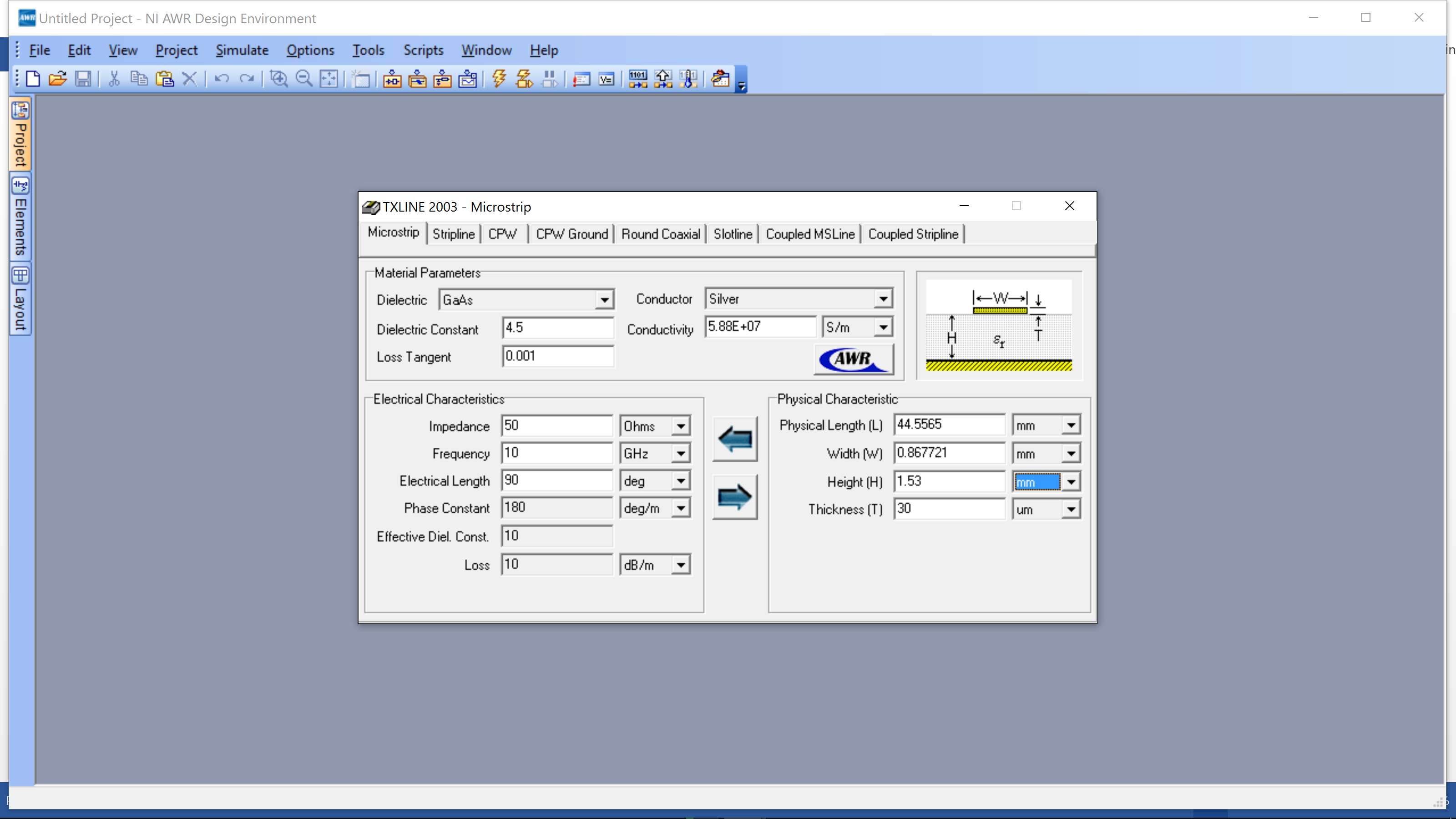
The picture shows a transmission line with a 50 Ohm impedance and an electrical length of 90 degrees at 950 MHz. The calculator works bidirectional. To find a transmission line from electrical length, insert all of the the parameters on the left. Also set Dielectric Constant=4.5, Conductor=Copper, Height=1.53 mm, Thickness=18um. These are obtained from the PCB stackup we are using in the workshop. Note that the Height and Thickness are set on the right side, even though we are calculating from left to right in this example. Click the right arrow – it will calculate the width and length to the line. Likewise, if you change the Length or Width on the right side and click the left arrow, it will calculate the new Electrical Length and Impedance. In the example above, it will calculate a 50 Ohm transmission line one quarter wavelength long (90 degrees) for the stackup seen on the right. Your numbers will be different due to stackup and frequency. Note 2.85 mm is approximately 50 Ohms for our stackup. In the kit, you received a 3mm copper foil, which is close to the 50 Ohm line.
Note that TX line id independent of your AWR design. You must enter in the calculated values into your schematic MANUALLY. It does not enter them for you.
Below is a video describing the design and layout of the direction al coupler. You should design it for -15dB split to feed to the branchline mixer.
Fabrication
The directional coupler is fabricated using the 3mm copper foil in your kit. Below is an example of how this is done for the impedance synthesis PCB. The same approach is used for the directional coupler.
The kit only comes with one 50 Ohm termination (in teh VNA calibration). If you do not have another, please solder a 50 Ohm resistor on the unused trace of the directional coupler (the one on the lower right). You can solder the resistor on over the board edge as shown below.

Testing
To test the coupler, connect that VNA to the input (port 1 out of VNA).
To test the through (S21), connect the 50 ohm termination (the “load” calibration) to the coupled port and the second port of the VNA to the output. See the image below. Note we used a second 50 ohm termination for the 4th port. In your design you should solder a 50 Ohm resistor (included in the kit) from the 4th port to the ground plane beneith. Simply solder it across the board edge.

To test the directional port, connect the 50 Ohm termination to the output and port 2 of the VNA to the directional port as shown below.

The measured results are shown below.
