Power amplifier
Design and Simulation
PA Core DC Bias
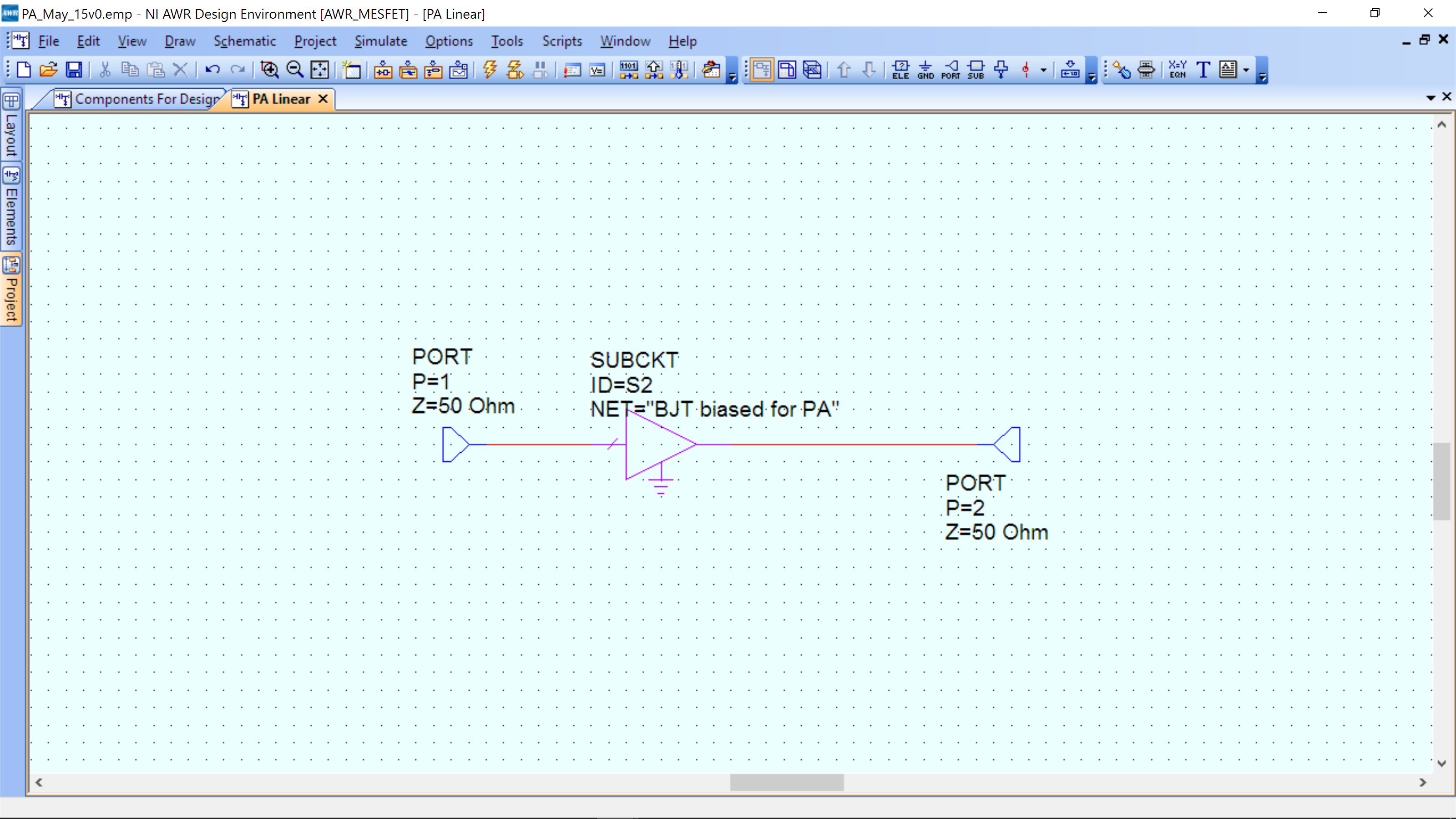
The basic amplifier schematic is shown below and can be found in the circuit design template as BJT Biased for PA. The currents are shown for a 75k Ohm bias resistor. We have found a 10k bias resistor produces more power and recommend it for design. The BJT Biased for PA has that 10k resistor in it already.
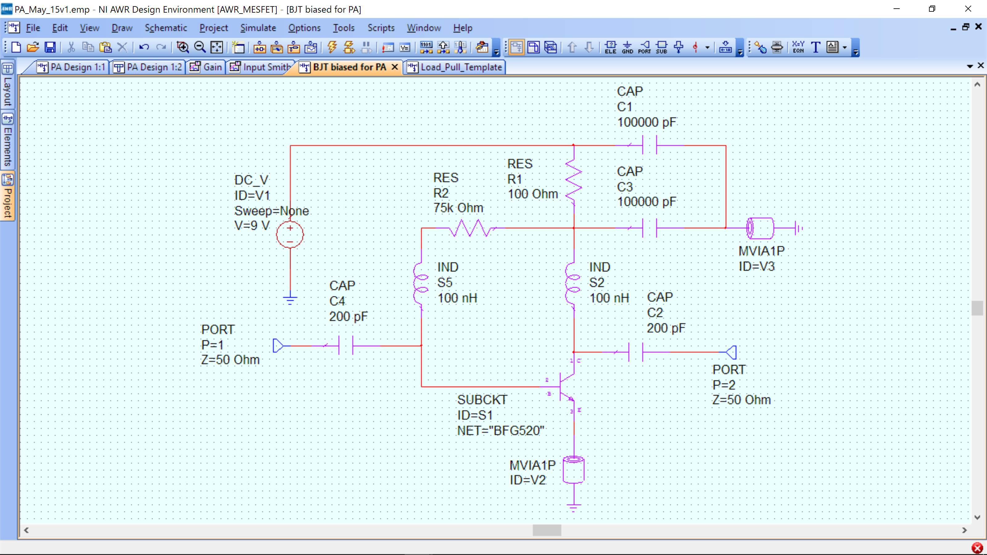
Component operation:
- R1, 2 – base bias current. (Minor collector feedback via R1, but this is only at DC due to C3). Base current is approx. Ib(9-.7)/75k.
- C1,C3 – decoupling capacitors
- S5 – decoupling inductor (choke) for base
- S1 – BFG520 BJT transistor
- S2 – Inductor – RF choke
- C2, C4 are DC blocking capacitors
- V2,3 are vias for our substrate.
- PORT 1 – input of amplifier core
- PORT 2 – output of oscillator core.
The DC bias conditions for the oscillator core are shown below:
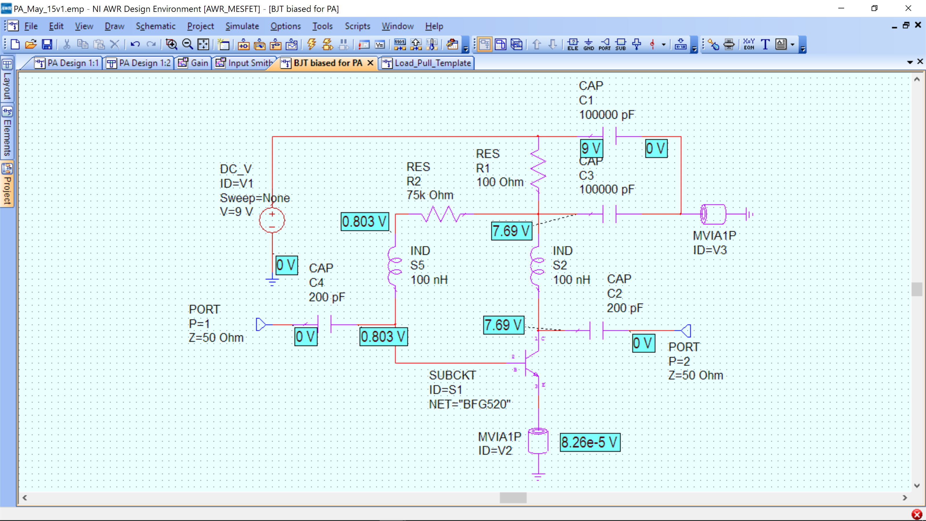
Collector current is 13.1 mA (not shown) and base current is 100 A.
Note that the voltage on R2 is reduced by approximately 1.3V due to the collector current through R1. This is due to feedback of the bias circuit which reduces the base drive as the collector current increases, thus ensuring that the DC bias current is not too large.
PA Core AC Gain
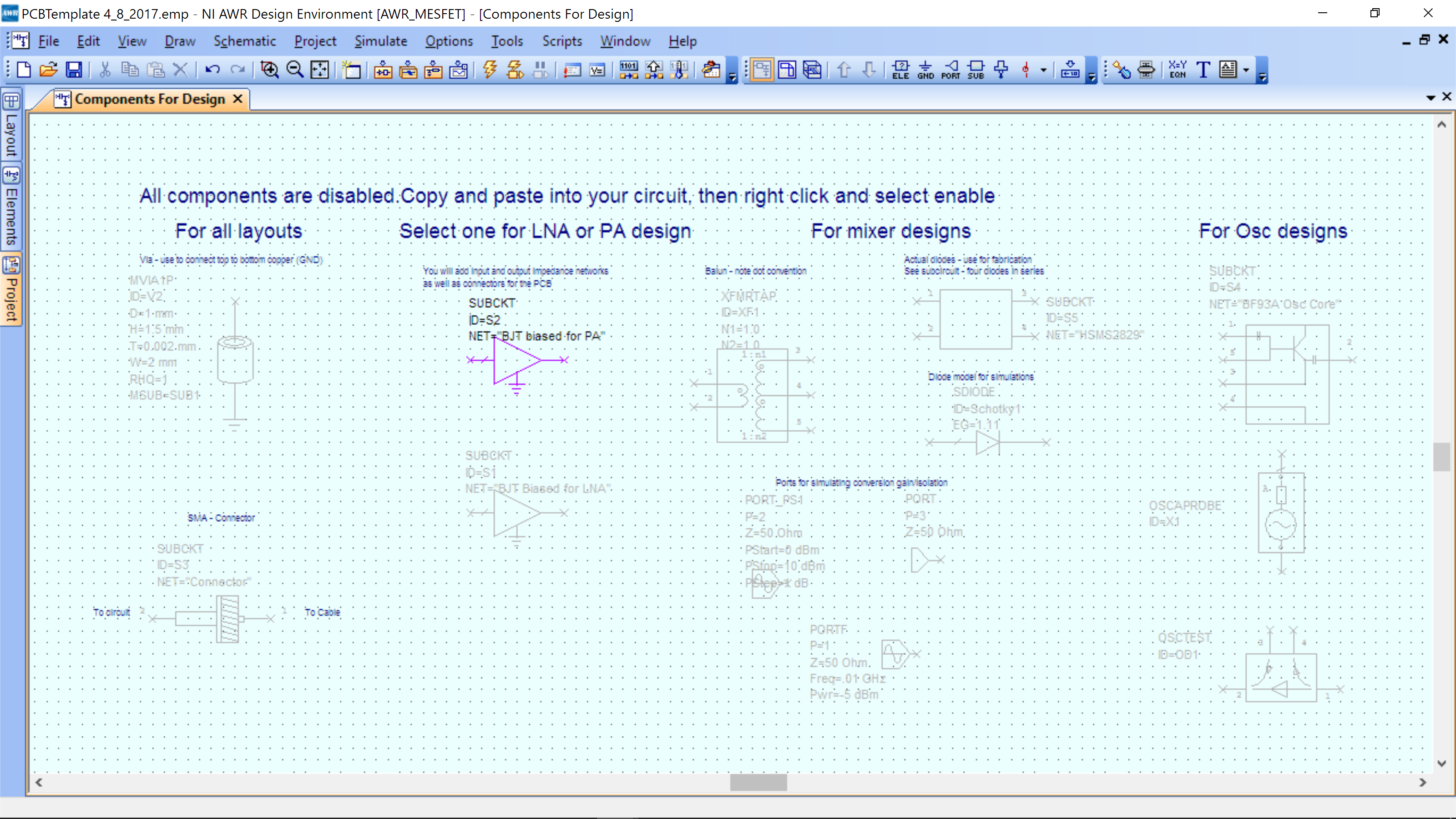
The following are the components we will use from the template. They have been enabled (Right-mouse Click->Enable) to be visible.
The first step is to measure the linear gain of the PA core.
Create a new schematic, Project -> Add Schematic. Name it “PA Linear.”
Insert the BJT Biased for PA by copying it from the “Components for design” schematic. Make sure it is enabled (right mouse click, then enable). The components on the design schematic are by default disabled (grayed out). Go back to the components schematic and disable the BJT biased for PA to ensure there are no problems during simulation.
Configure as below for AC testing.
Components can be added as follows:
- PORT and GND can be added directly from the tool bar at the top of the software (labeled “PORT” and “GND”)
- All other elements can be added by Ctrl+L then type the name of the element, e.g. RES or CAP, and you will find it in the list that appears.
- You may rotate and flip components by selecting them, then Right-mouse Click->Rotate or Flip
- Special components: MVIA1P (special via to ground) must be copied from the Design for Components Schematic in the template provided.
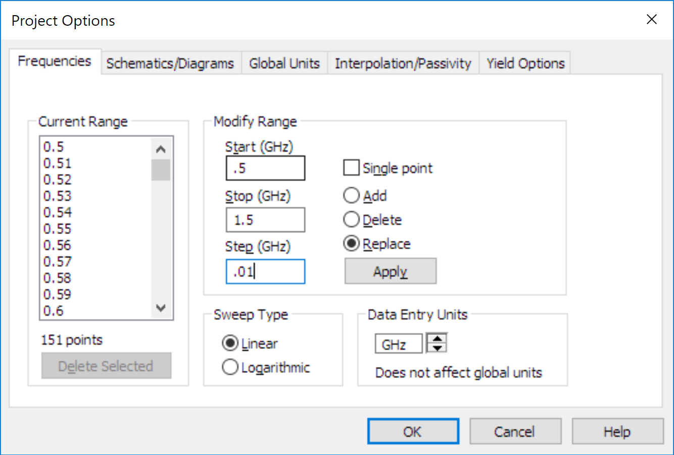
Setup the simulation by going to Options->Project Options->Frequencies and setting the range from 0.5 to 2 GHz in 0.01Ghz steps. Hit Apply and make sure replace is selected.
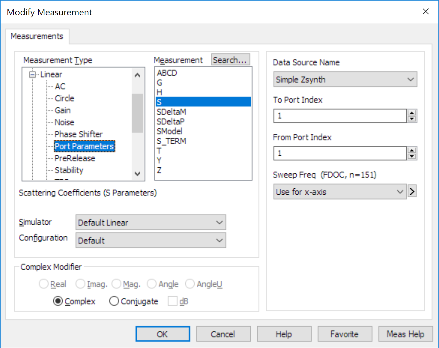
The measure the gain (S21), both in magnitude and phase. Click Project->Add Graph. Name is something useful, e.g. PA Linear Gain, and make sure Rectangular is selected for the plot type. Once the graph is created, Right Mouse Click->Add New Measurement. The following window will appear:
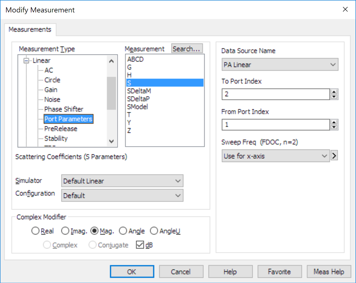
Ensure that the Data Source Name is the design you want (not All Sources), then select Port Parameters->S then select 2 and 1 from the port indices. Select Mag and dB. Hit Apply.
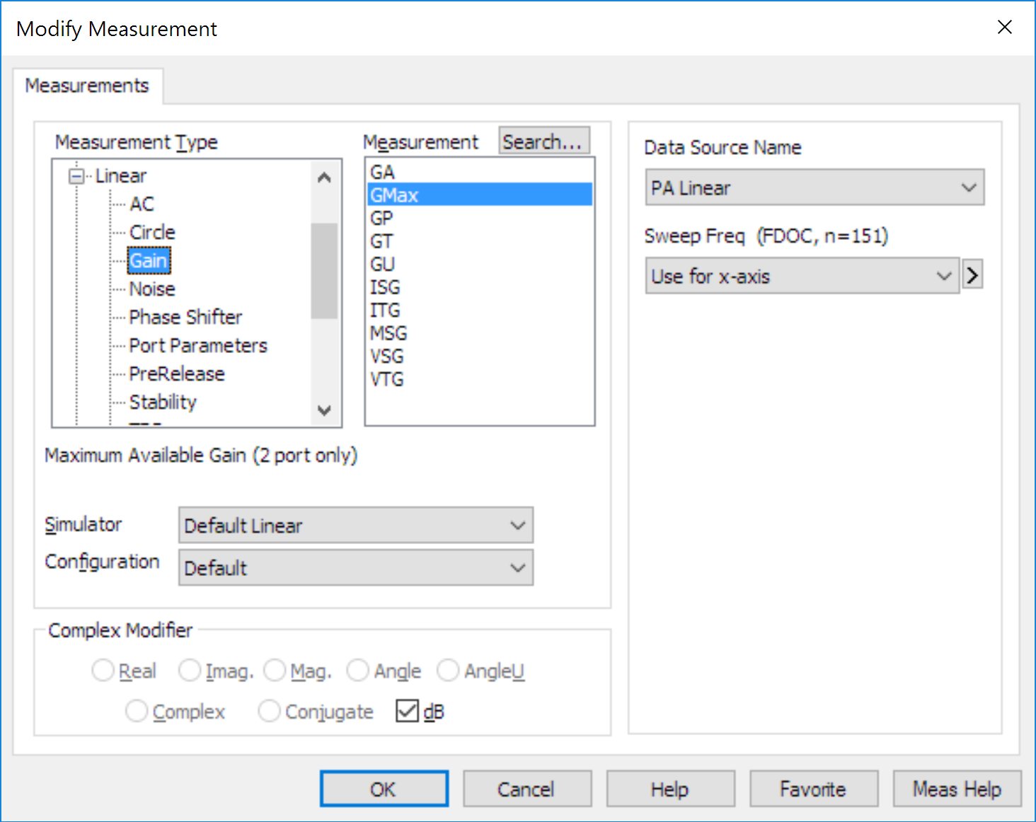
Also at Gmax which represents the maximum linear gain possible if the core was complex-conjugate matched.
You can simulate your design by clicking the lightening bolt on the top menu (Go to Simulate->Analyze to simulate and see an image of the lightening bolt that also appears on the top menu).
The results are below. You can add a marker by Right Mouse Click->Add Marker.
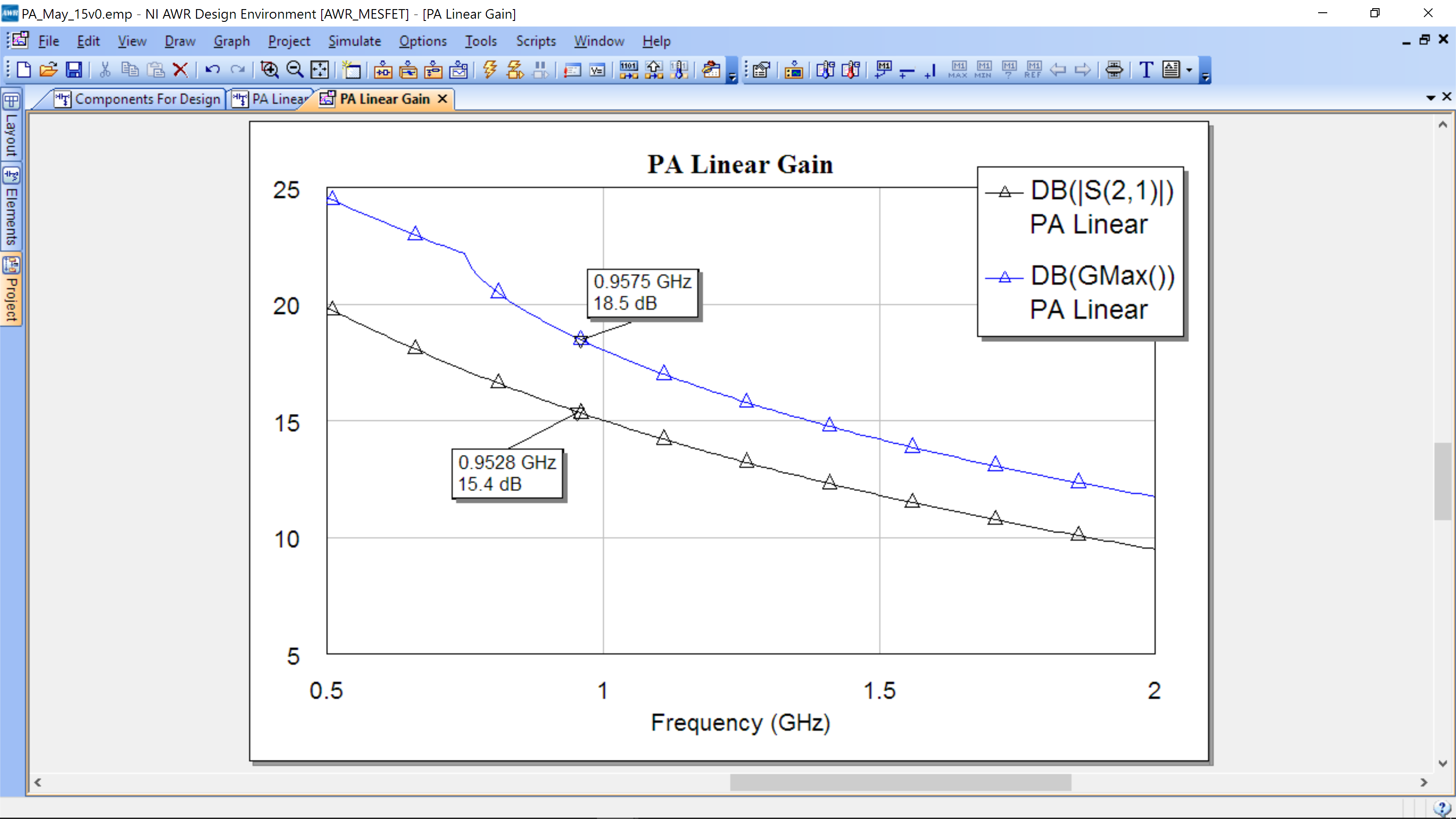
This shows the gain with 50 Ohm ports at the input/output and also the potential gain if the input/output were bi-conjugate matched. These are for small signal only, however. As soon as we increate the output power, and the amplifier moves into a non-linear regime, the gain and power will be very different.
Performing Load Pull
Unlike small signal (linear) conjugate matching, when the amplifier is operated in a non-linear regime, e.g. Class-AB, the definition of a small signal impedance becomes ill-defined. We no longer ask “what is the output impedance of the amplifier” in order to find a conjugate match (as we would do for a linear amplifier), but rather ask the question: “What load impedance maximizes the output power and/or PAE.”
To answer this question, we run a Load-Pull simulation, which basically tries, systematically, different impedance on the amplifier output and calculates the resulting output power and efficiency. From microwave theory, we find that the output powers and efficiencies will appear on circles of impedance, such that any impedance on that circle would produce the same power or efficiency. This will become clear when we perform load pull on our circuit.
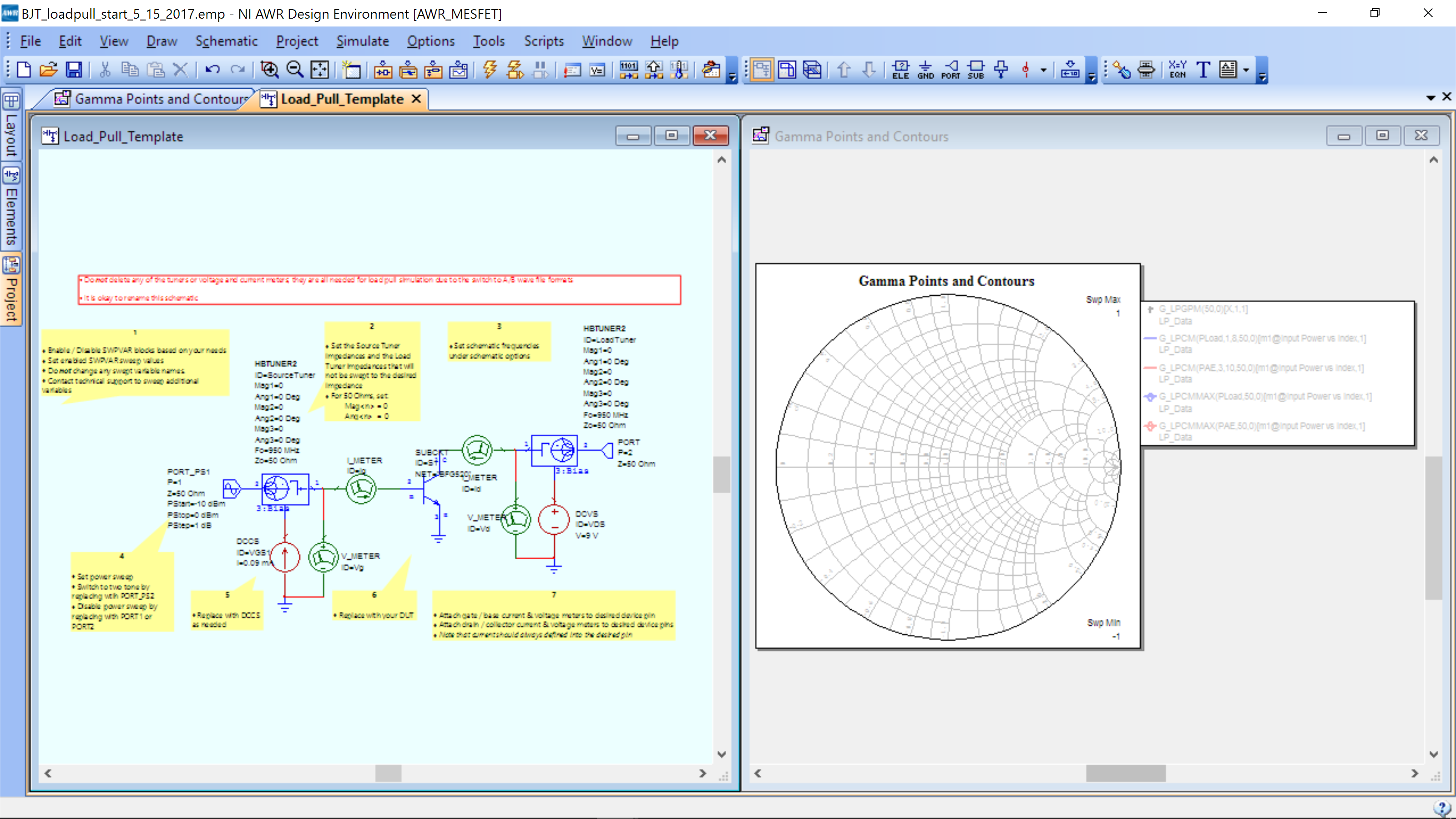
In the files you downloaded from the template menu page, open the file “BJT Load Pull Start ###”, where ### is the number of the transistor you wish to use (550 is for 950 MHz.)
You should find this schematic Load Pull Template:
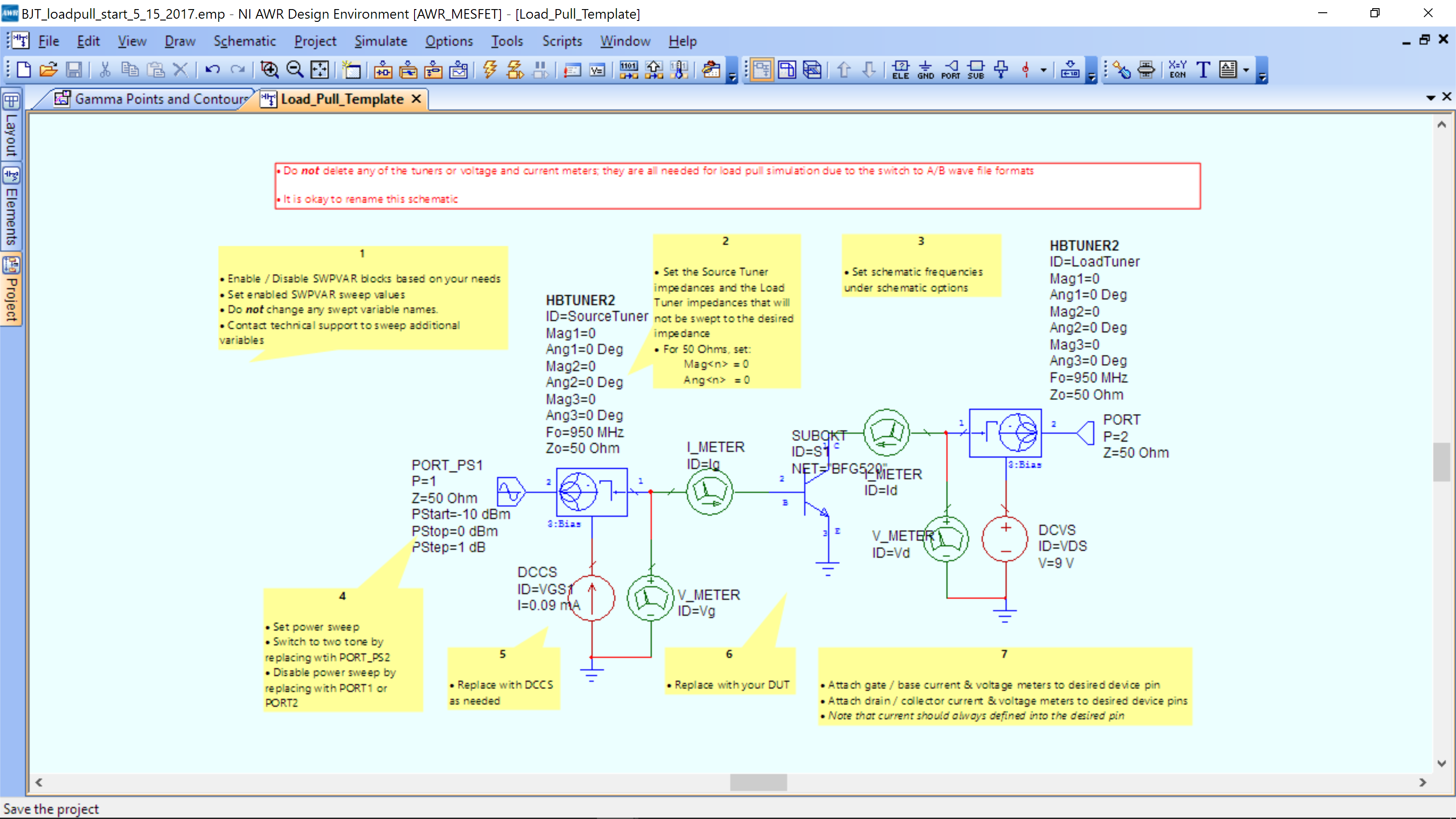
There is nothing for you to modify or change on the Load Pull Template.
For reference (do not do this step) – the template was created by going to; Scripts->Load Pull->Create Load Pull Template. After this was done, the transistor was changed to the one used in our workshop and the bias current set to the DC currents for our core and supply voltage of 9V.
The load pull template consists of an input and output network with the same functionality. They provide the DC bias points (voltage and current) and then an impedance “tuner”, HBTUNER, that will step through impedance both on the input and output of the transistor. By setting the correct bias condition, we will ensure the transistor is operating in the correct mode, i.e. Class-AB.
The procedure is as follows:
- Assume a 50 Ohm source impedance.
- Sweep output loads to find optimal power and efficiency
- Set output impedance to optimal value.
- Measure input impedance
- Provide a conjugate input match.
- Re-run load pull
- Iterate as desired (once is usually enough.)
Run the load pull from the top menu: Scripts->Load Pull->Load_Pull.
The following appears.
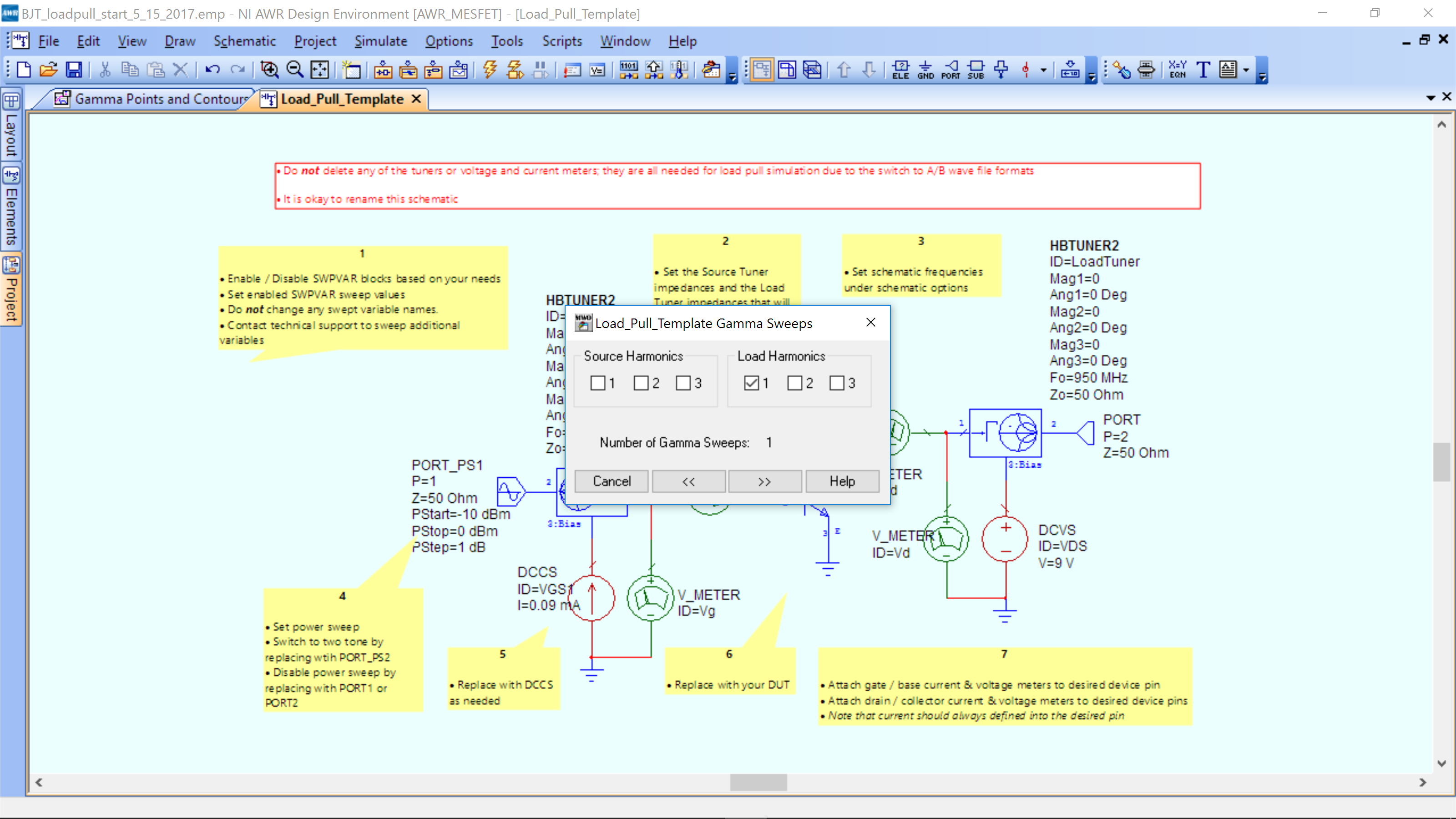
Leave selected that it will sweep only the first harmonic of the load and no harmonic of the source. Click the >> to advance the menus.
The following window(s) will appear:
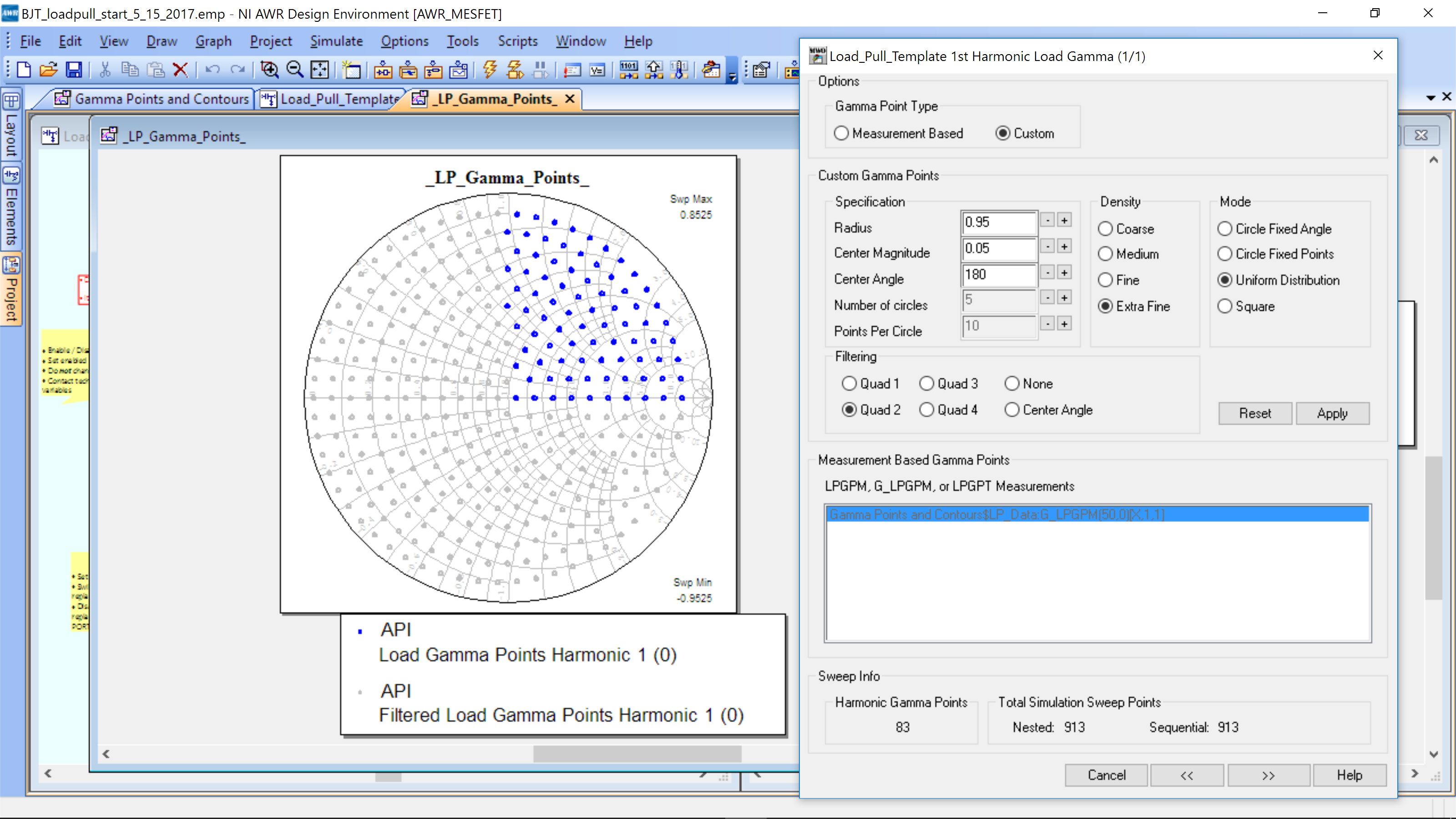
You can select the space over which to sweep the load impedance. It should be set to sweep in Quadrant 2 of the Smith Chart (this quadrant is chosen based on design history with the part). The LP_Gamma_Points shows the impedances that will be swept. Click >> to advance the menus.
The following will appear:
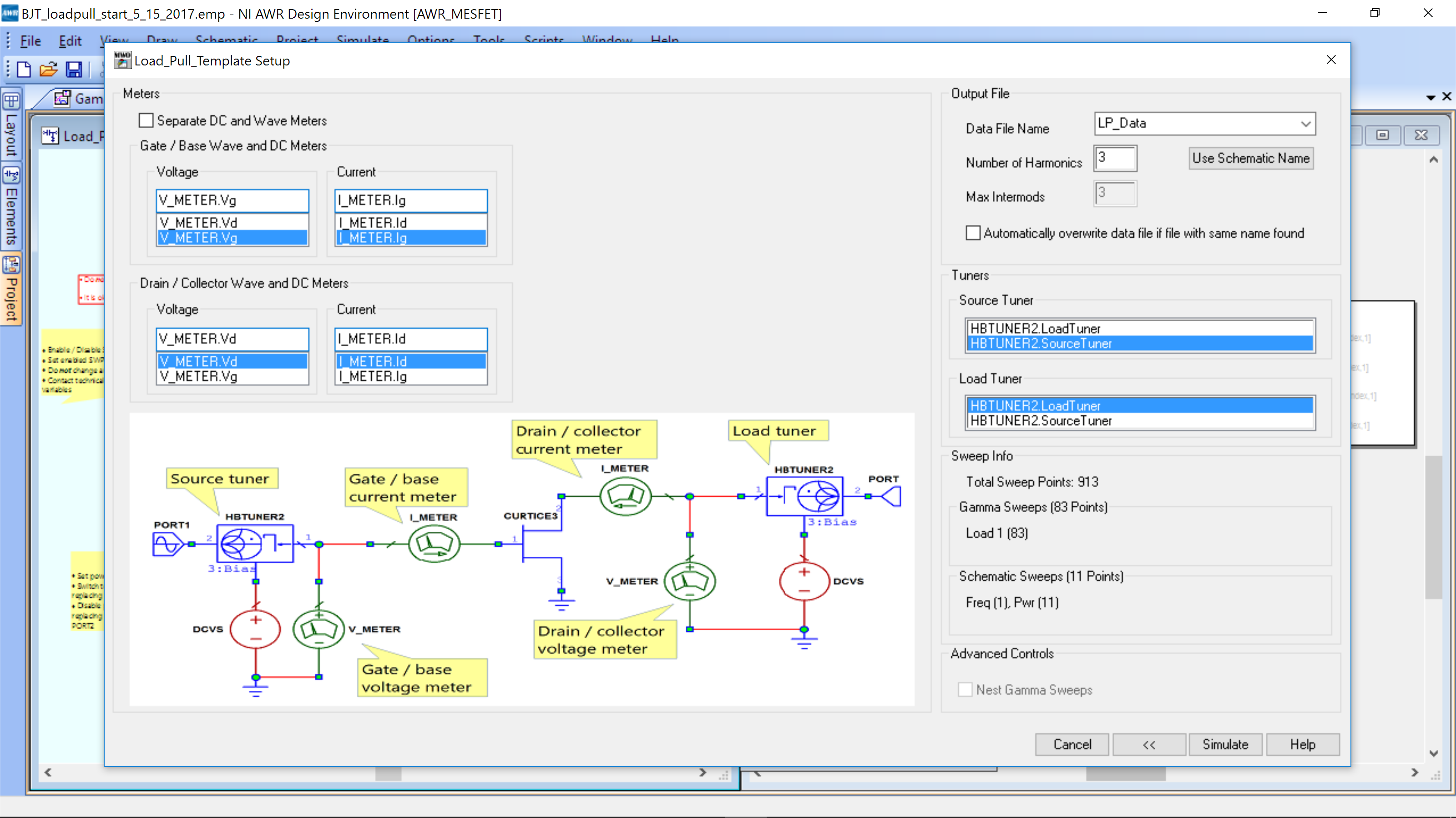
You do not need to make any changes. Click Simulate. Click OK to overwrite any files. Load pull will complete and the following should appear. If not, you can open both from the Project tab on the left. Use View->Tile Vertically to arrange.
Now Analyze (lightening bolt). The Smith Chart on the right will be populated (it was pre-setup in the template file to save you time and errors in setting up).
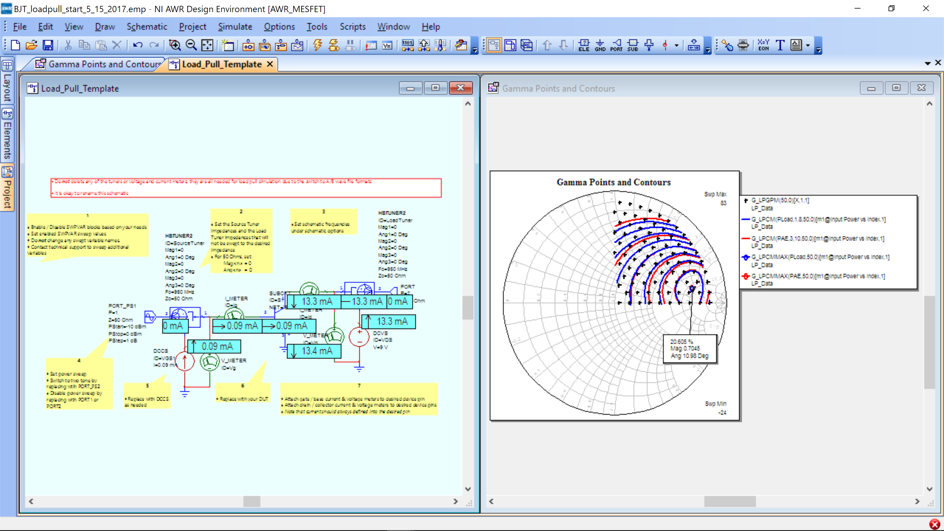
We can see the constant power and efficiency circles. The markers show the maximum for both efficiency and power. The crosses show the load-pull points. Maximize the Smith Chart window, then double click on the cursor. The following should appear:
And the label will show you the impedance at the maker. It is not shown here as it is your design choice/goal. The maximum power at this point is approximately 14 dBm (dBm is dB relative to 1 milliWatt.)
We sill use the maximum power point as the target load impedance seen by the PA, ZL=R2+X2j, where R2 and X2 are the real and imaginary parts of the maximum power point in load pull. Note: They are not the complex conjugate of any impedance and are not determined by the small signal output impedance of the PA. Instead, we directly swept load impedance to find the one that produced the maximum power.
You will note in the legend that it says “G_LPCMMAX(Pload,50,0)[m1@Input Power vs. Index,1]. This indicates that the plot is for the input power at power input=index 1. To find out what that power is, simple return to the Load_Pull_Template and look at the input port, PORT_PS1. It sweeps from -10 dBm to 0 dBm in steps of 1 dB. The plot is setup to use the input power marked by a marker on a hidden graph. We have provided an easy way to see this. Go to Project Tab->Graphs-> Input Power vs. Index. The following should appear (we have closed the Load_Pull_Template schematic and tiled the windows vertically).
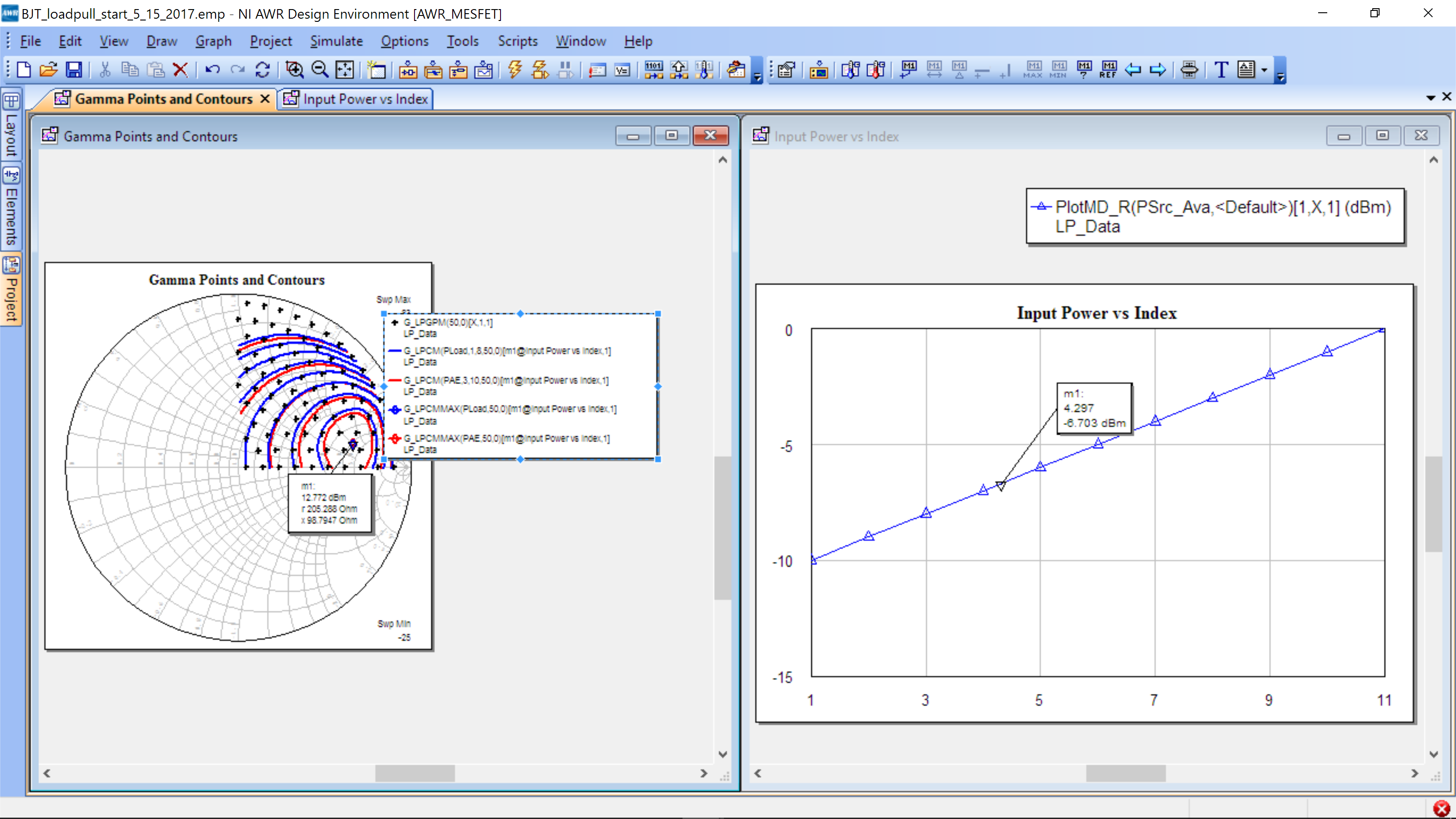
You can see the cursor M1 on the right. As you move the cursor, you will see the load pull on the left change. This means that the optimal load impedance is dependent on the input power. The loadpull template us set to -5 dBm as the default input power, however you can choose a different input power around which to optimize.
Return to the PA Linear schematic (not in the load pull template, but rather the first schematic you made). Trick: You can double click the “50 Ohms” in the output port of your AC simulation and enter in the impedance that you found in load pull. Here is an example of entering 100+90*j (not the optimal point).
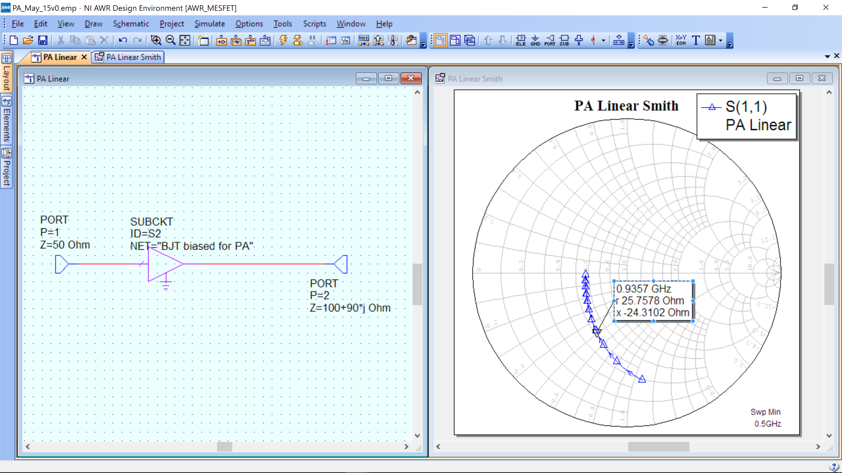
Also shown is a Smith chart plotting the input impedance (S11). This graph can be added by Project->Add Graph->Smith. You can name it “PA Linear Smith”, then Right-mouse Click->Add Measurement and add an S parameter measurement as before, but select complex on the lower left.
You can now measure the input impedance. For this workshop, we will use a simple conjugate match for the input. The impedance seen by the PA input will be ZS=R1+X1j, where R1 is the real part of the PA input impedance and X1 is the complex conjugate of the PA input impedance. In an optimal design, we could reiterate with the new source impedance to find a slightly better load impedance. Or we could do a full source-pull with out load-pull, searching for the best source and load impedance.
We now have a desired load impedance (from load pull) and source impedance (from a linear Smith chart measurement with the output terminated with the desired load).
Synthesizing Impedances
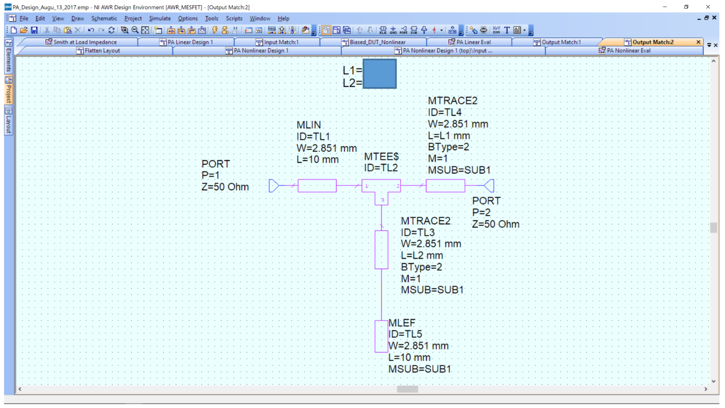
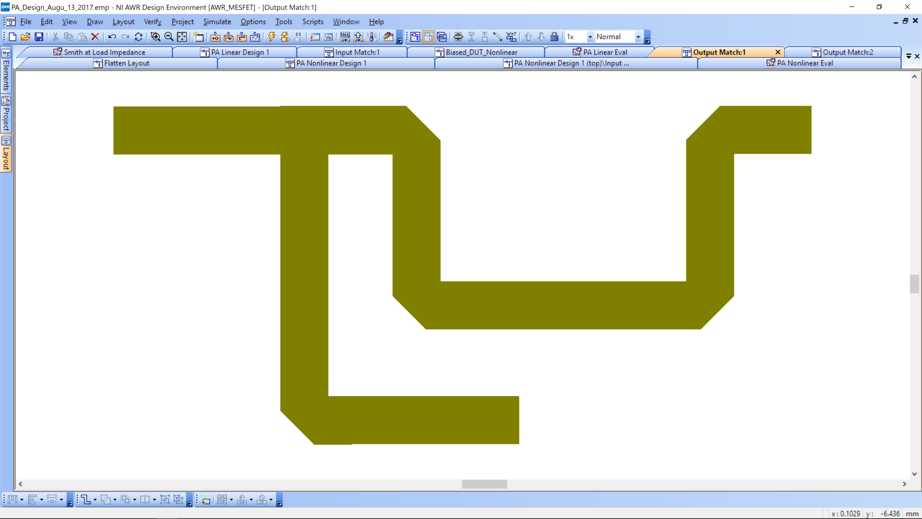
To synthesize the impedances, we will take a short-cut and assume a topology for our impedance synthesizer and simply “tune” it to give us the impedances we need. Below is a picture of the two impedance synthesis networks. The one on the left impedance transforms 50 Ohms to the target impedance for the input of the PA (the complex conjugate of the PA input impedance, ZS=R1+X1j). The one on the right impedance transforms the 50 Ohm load to the target impedance of the PA output (this is the value found during Load-Pull, ZL=R2+X2j).
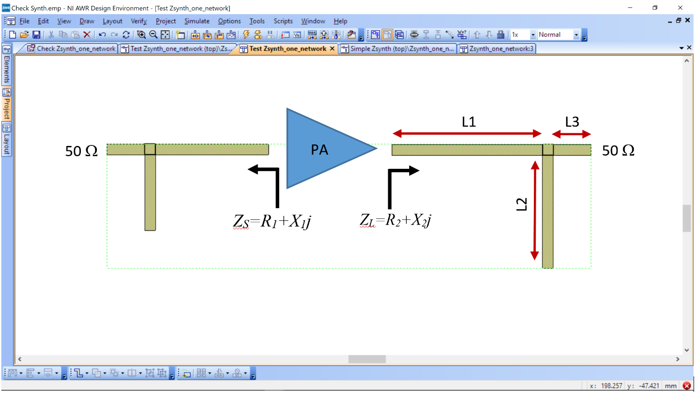
We will demonstrate how to design the right imepdance matching network for ZL. The same procedure can be used for the left, or input matching load.
There are three transmssion lines of lengths: L1, L2 and L3. All are 50 Ohm transmission lines (2.85 mm width using our PCB). L3 is a 10 mm long transmision line used to connect to the 50 Ohm SMA connector. Its length does not change. L1 connects to the PA output and the junction of the three transmission lines. It will be adjustable in length. L2 intersects between L1 and L3 and is open at the other end. It is an open “stub.”
The impedance transformation is done by varying L1 and L2, such that the impedance looking into L1 at the left equals the target ZL.
Create the following schematic for the impedance transformation network. For convenience name it OutputMatch. You should create a second schematic named InputMatch. Both have the same schematic, but different values of L1 and L2.
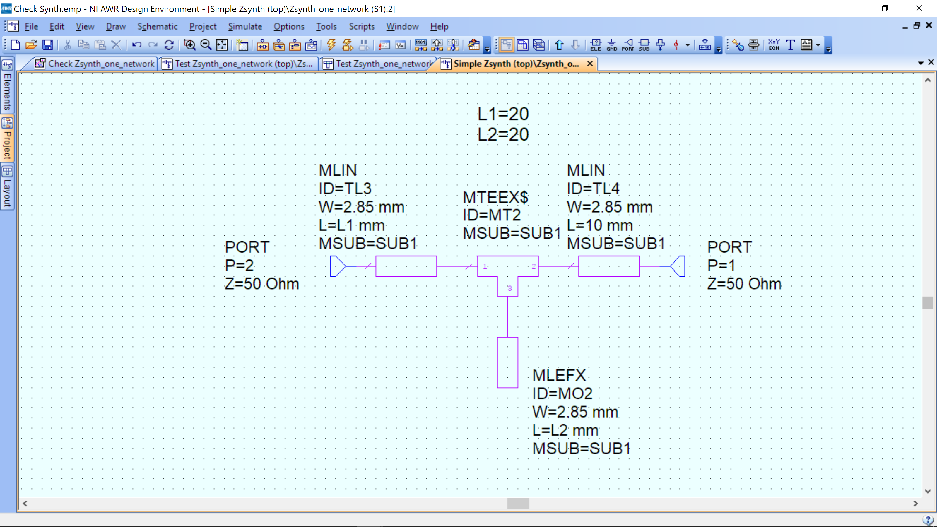
MLIN can be created using Ctrl-L then typing MLIN to find component. MTEEX$ is a “T” junction that will automatically size to connect to line widths at its ports 1,2 and 3. Since these lines are all 50 Ohm, the widths are the same. MLEFX is a transmission line that is open at one end. The EM model properly models the open end. If we simply used MLIN and didn’t connect one end, the EM model would not properly model it.
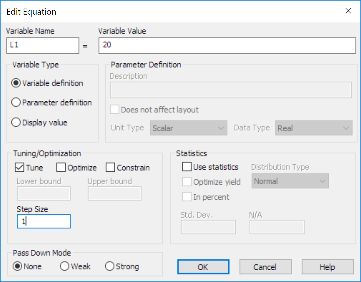
Use Ctrl+E and click anywhere above the circuit and an equation will appear. Type L1=20 and L2=20. Then enter the lengths of the left and bottom (open stup) transmission lines as L1 and L2. The units are determined by the component (mm). Now, on each equation Right Click -> Properties and then click tune and enter step size as 1 as shown below.
The equations will turn blue in the schematic to show they are now tunable. Projects -> Add New Graph, label “Output Impedance Transformation” and select Smith Chart. Right Click -> New Measurement and add S11 and S22 as complex impedances as shown below.
Make sure Data Source Name is set to your schematic name. In this example, we named our schematic “Simple Zsynth.” If you haven’t set frequencies, go to Options->Project Options and set the frequencies below (make sure to select and click Replace).
Now run the simulation by clicking on the lightening bolt icon found on the icon toolbar at the top of the window. It will be under the Tools and Scripts text menu labels. Your simulation should look like this. Note we have clicked the tune icon (upper right on icon tool bar) and a tuner window as shown up on the left. We have also added a marker (Right Click -> Add Marker) to show 950 MHz.
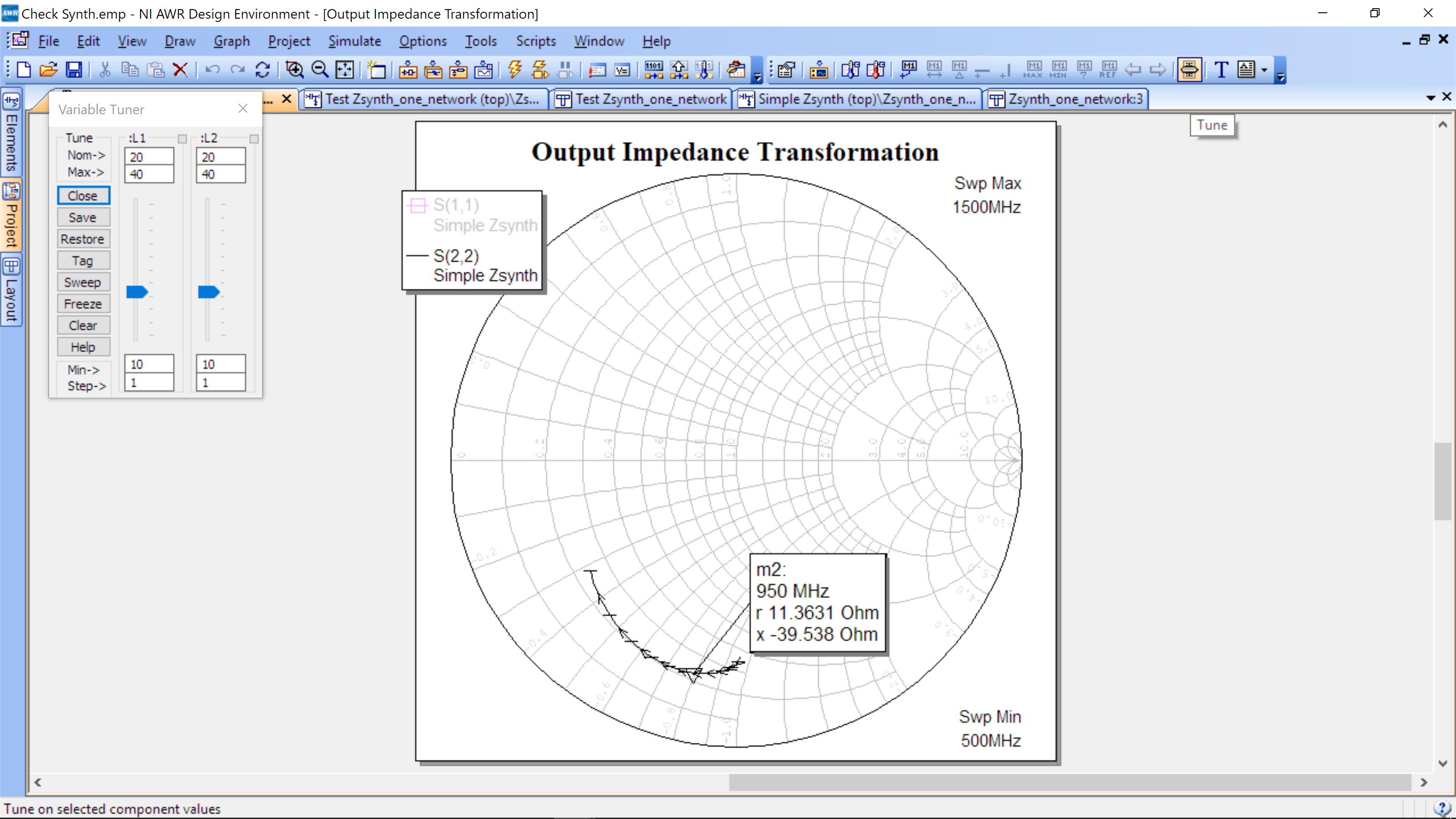
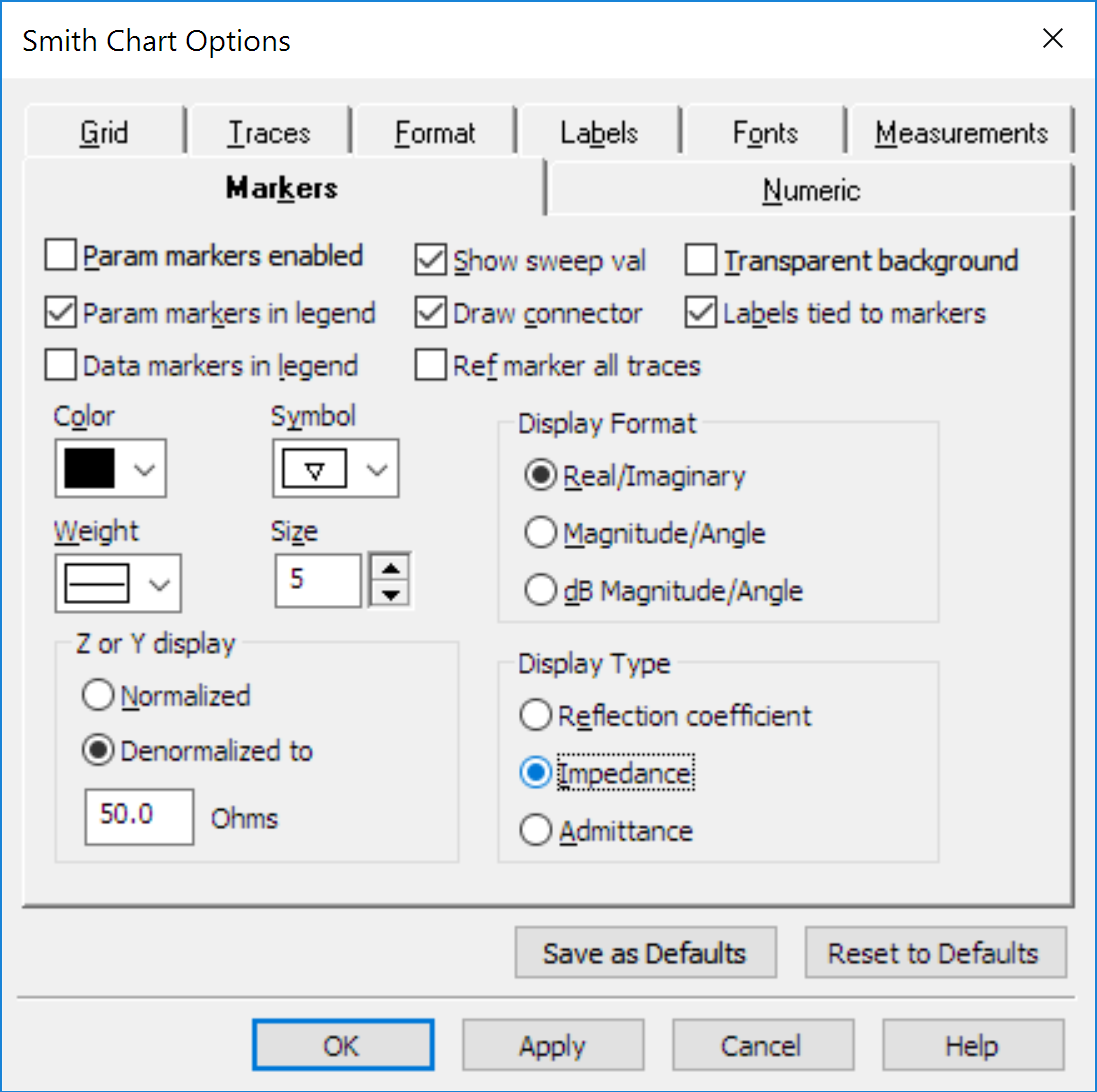
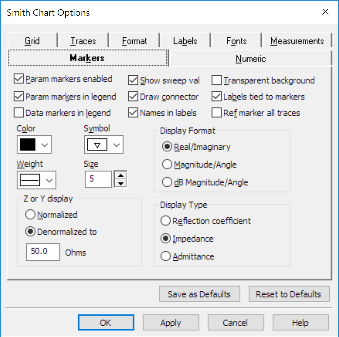
Double click the marker text box to ensure you have the complex impedance shown and Denormalized to 50 Ohms.
It is very important to know which impedance you are tuning. In the example, we are tuning S22 not S11 as Port 1 is connected to 50 Ohms and is not being adjusted. We are impedance transforming the 50 Ohms at Port 1 to the desired impedance. For example purposes, lets transform to ZL=100+50j.
Adjust L1 and L2 by sliding the tuner bars. You can extend the tuning range from 40 (set as default) to a higher value by changing the Max value under L1 and L2. You will clickly gain intuition on how the marker moves. After about 30 sec, we have achieved the following:
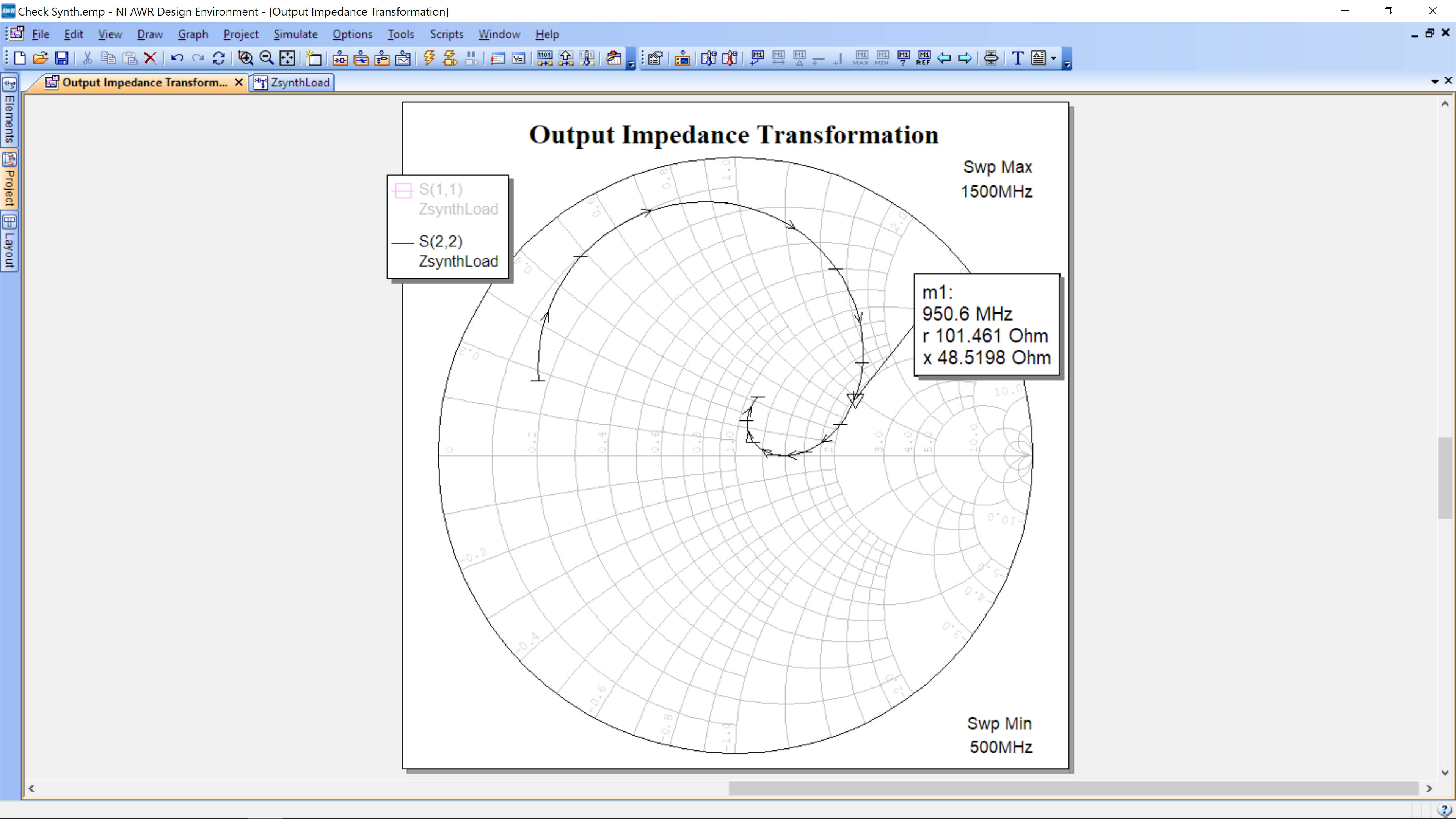
Which is close to our target impedance. We could modify the step size to below 1 mm to achieve more precision or simply use this as our impedance. It will be difficult to match exactly your target impedance with this network if you are far away from 50 Ohms as your target impedance.
You can now go to your schematic, View-> Layout and see the layout below. I have used Ctrl-A to select all then Edit->Snap Together to do an auto layout.
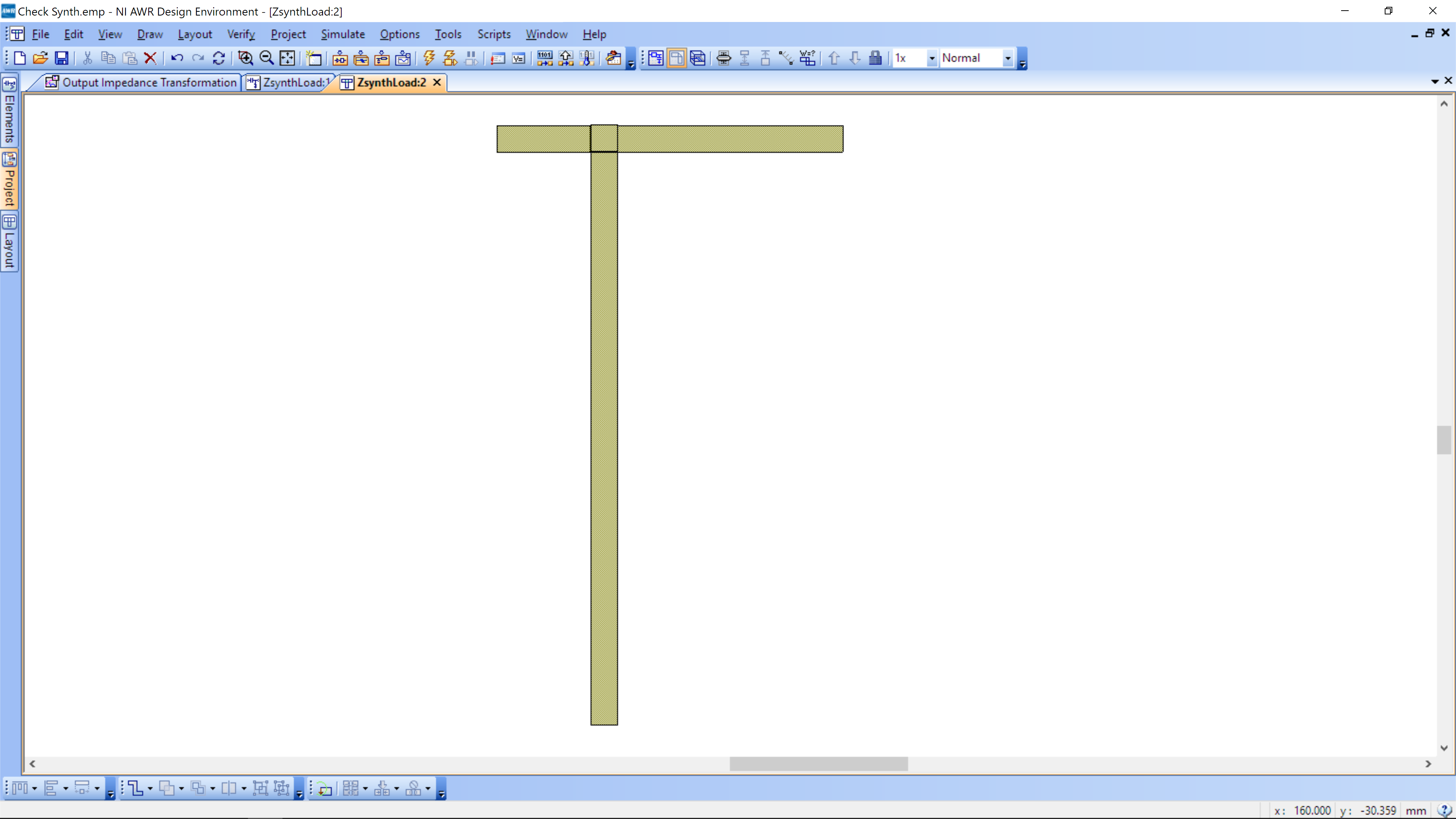
Note that the 10mm feed line is on the left in this layout, but for our PA, it would be on the right as that is the output.
You can repeat the design process for the input matching network.
Amplifier Design
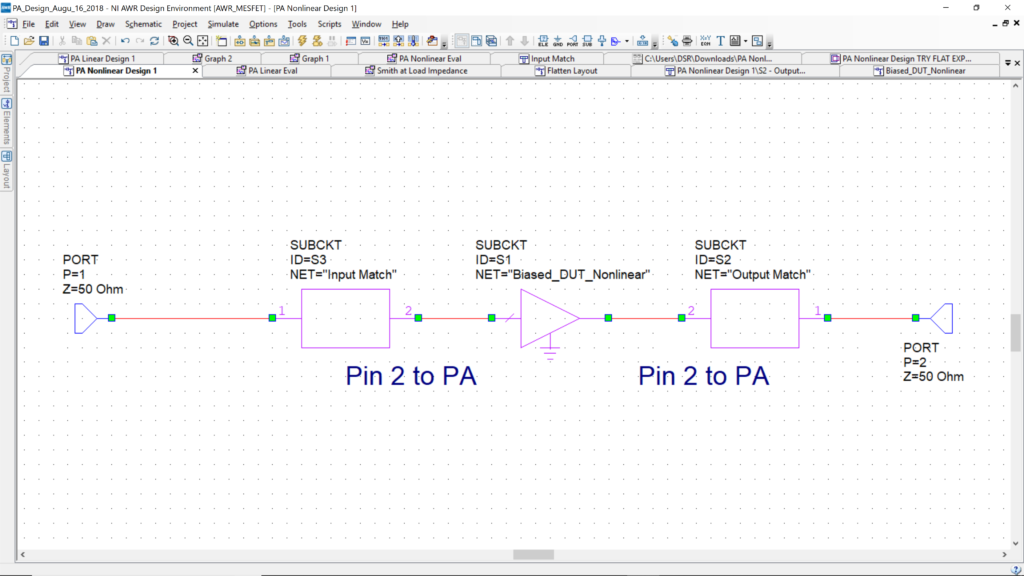
Assemble the following schematic. A symbol is made automatically for every schematic you make with ports. Just go to the left Elements tab, then open Circuit Elements and look for Subcircuits and click on that. In the subbox below, you will see a list of subcircuits, you should find the schematic you made for impedance transformation. In the example below, our output was called “OutputMatch” and the input “InputMatch.” The sub circuit block will match the pin “1” and “2” on the symbol to PORTS 1 and 2 of your subcircuit. Make sure
to connect the PIN 2 of the impedance transformers to the PA.
You can plot the gain (S21) and Gmax.
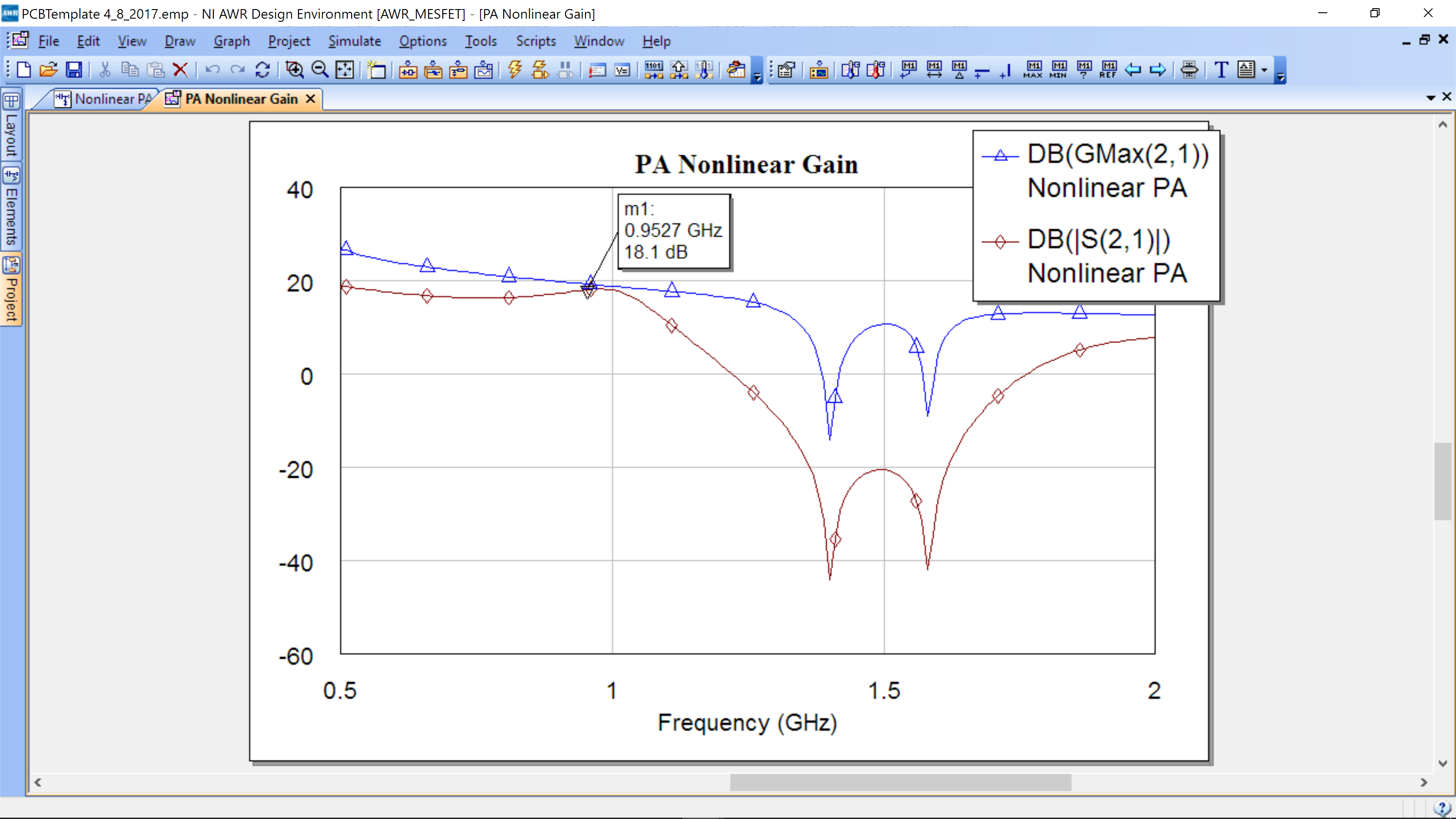
We can see that for small signals we are also well matched. To measure the output power, create a new schematic (call it Nonlinear PA 2) as below:
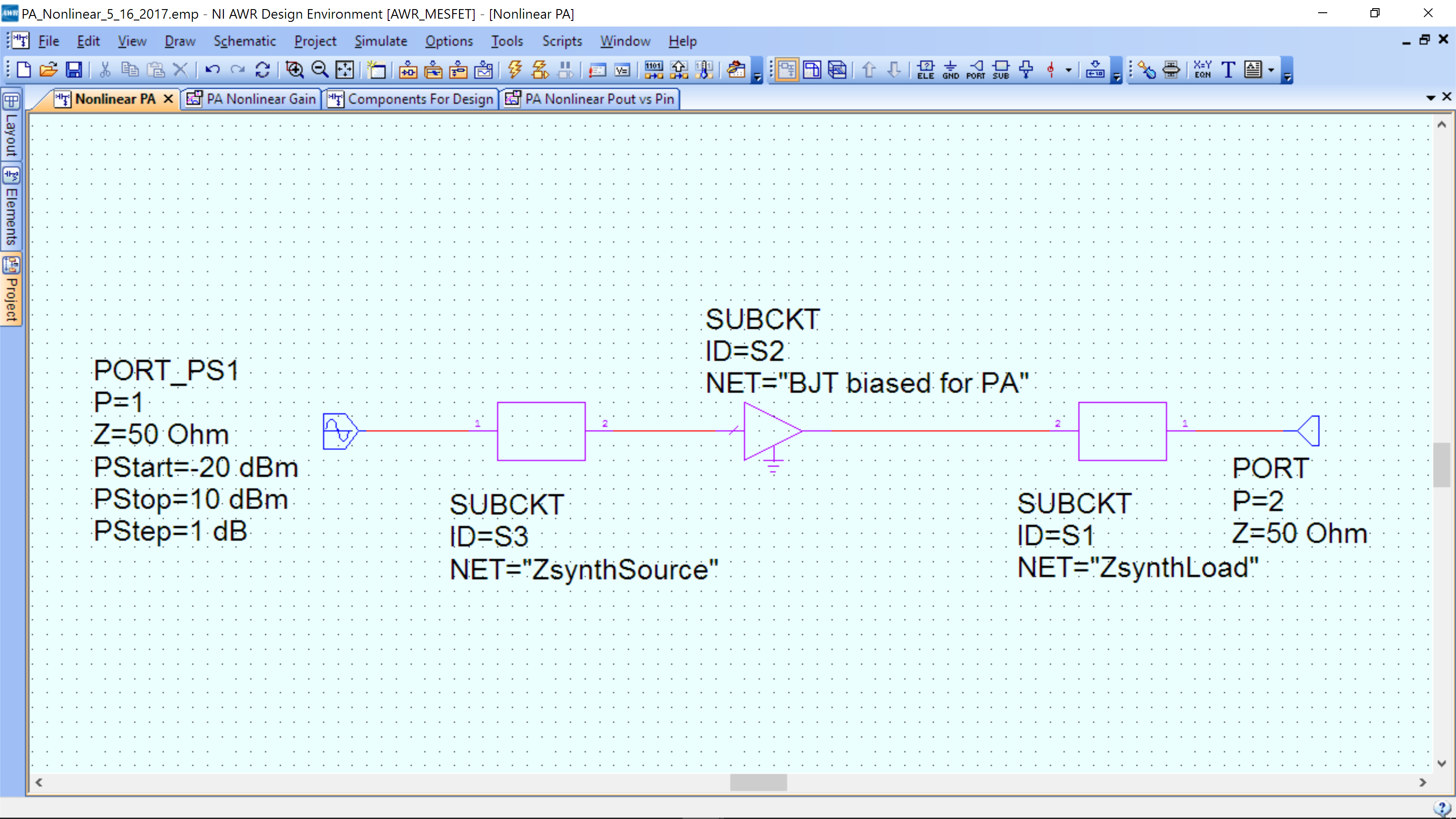
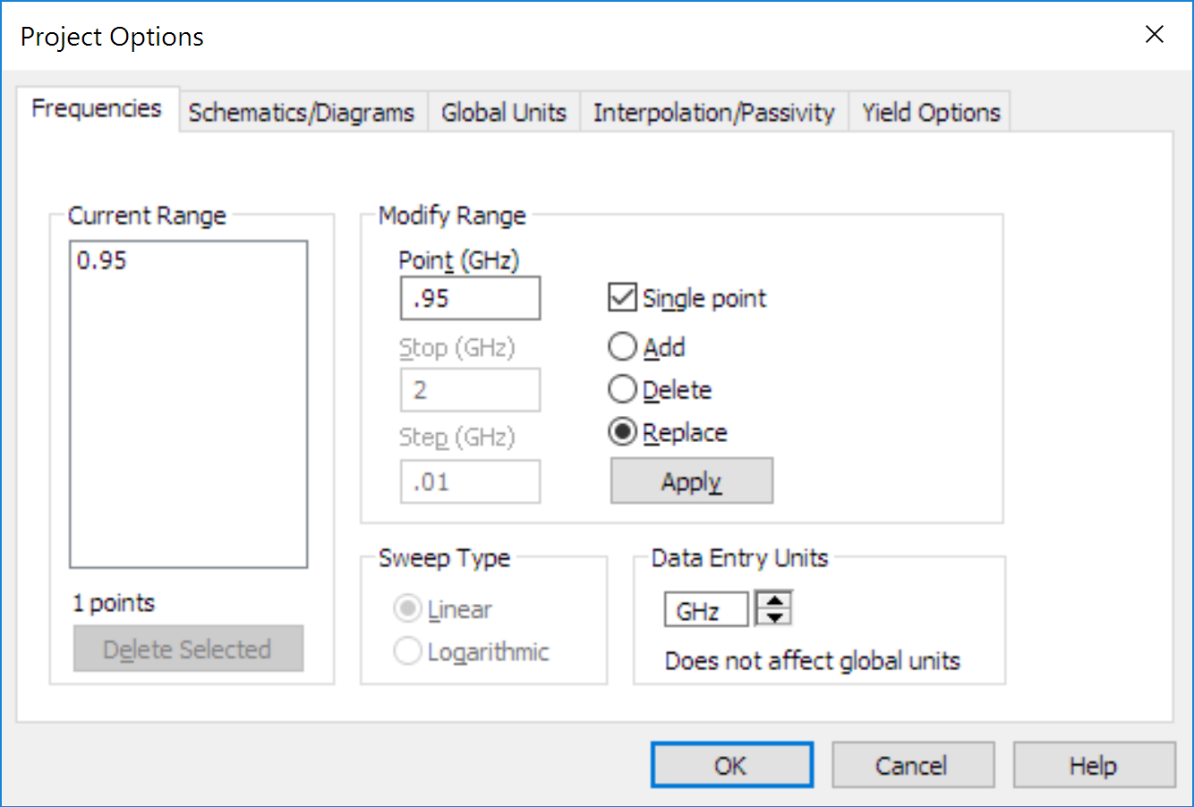
We have just changed the input port to PORT_PS1 and set the input power sweep to -20 dBm to 10 dBm. From the top menu, Options->Project Options->Frequency set to a single point at 0.95 Mhz.
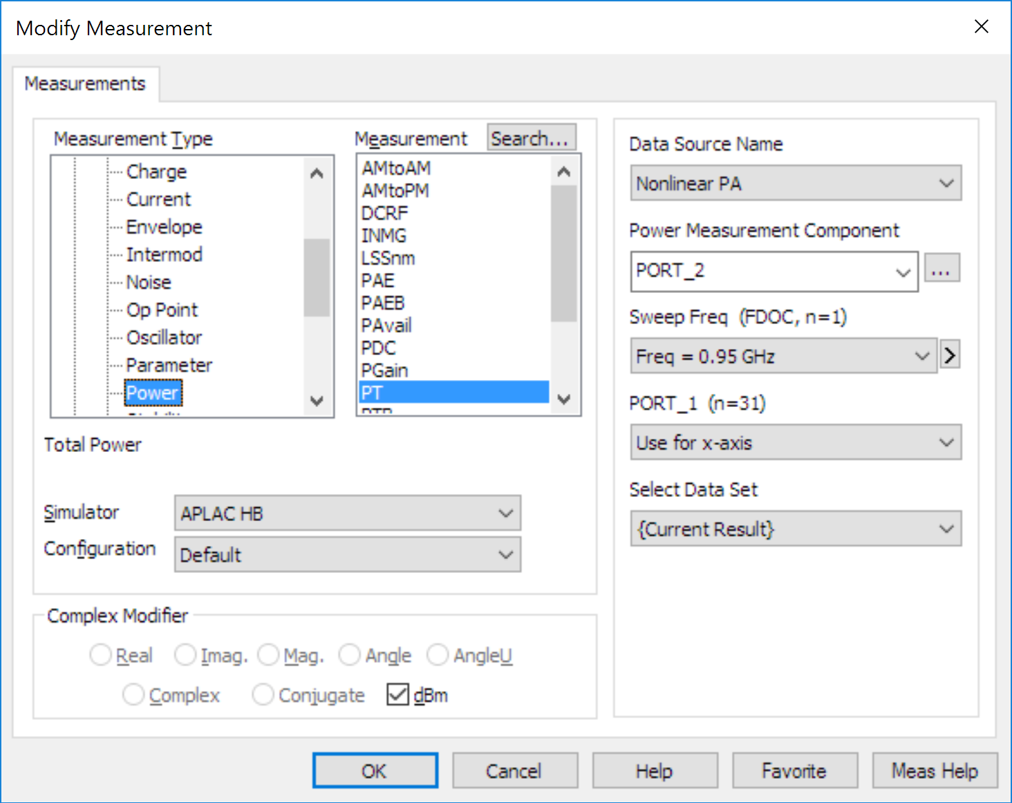
Insert a graph with the following measurement. Ensure that the Data Source Name is correct and the Sweep Freq and PORT_1 setting (you may need to scroll up to see Use for x-axis).
Simulate using the lightening bolt. The following is an example of the ouput.
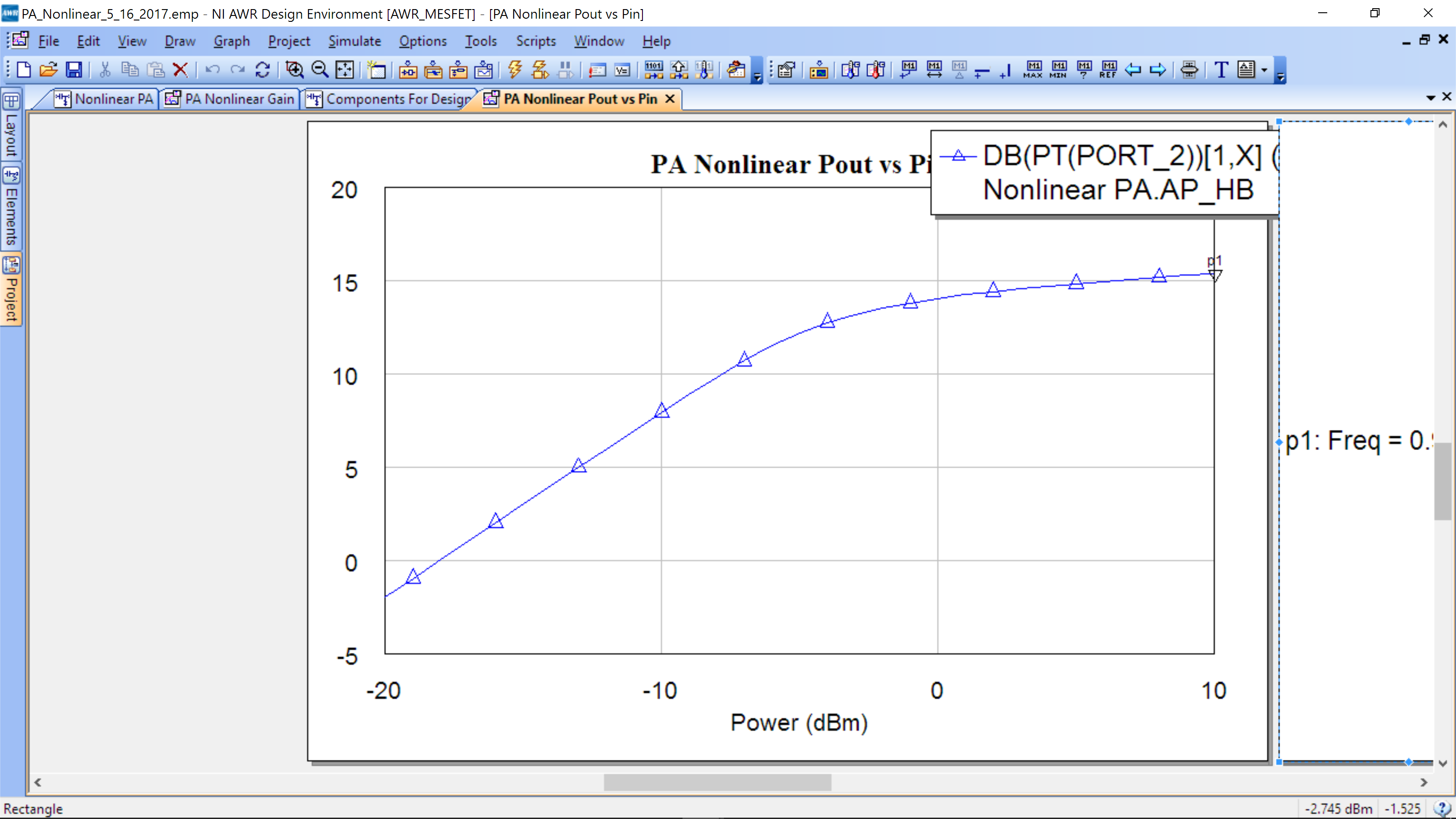
At -5 dBm input power, the output is around 12 dBm, as expected from our load pull. In addition, we can see that the power amplifier saturates much above 12 dBm output power.
Layout
While in the schematic for the PA, go to View-View Layout. The following will appear.
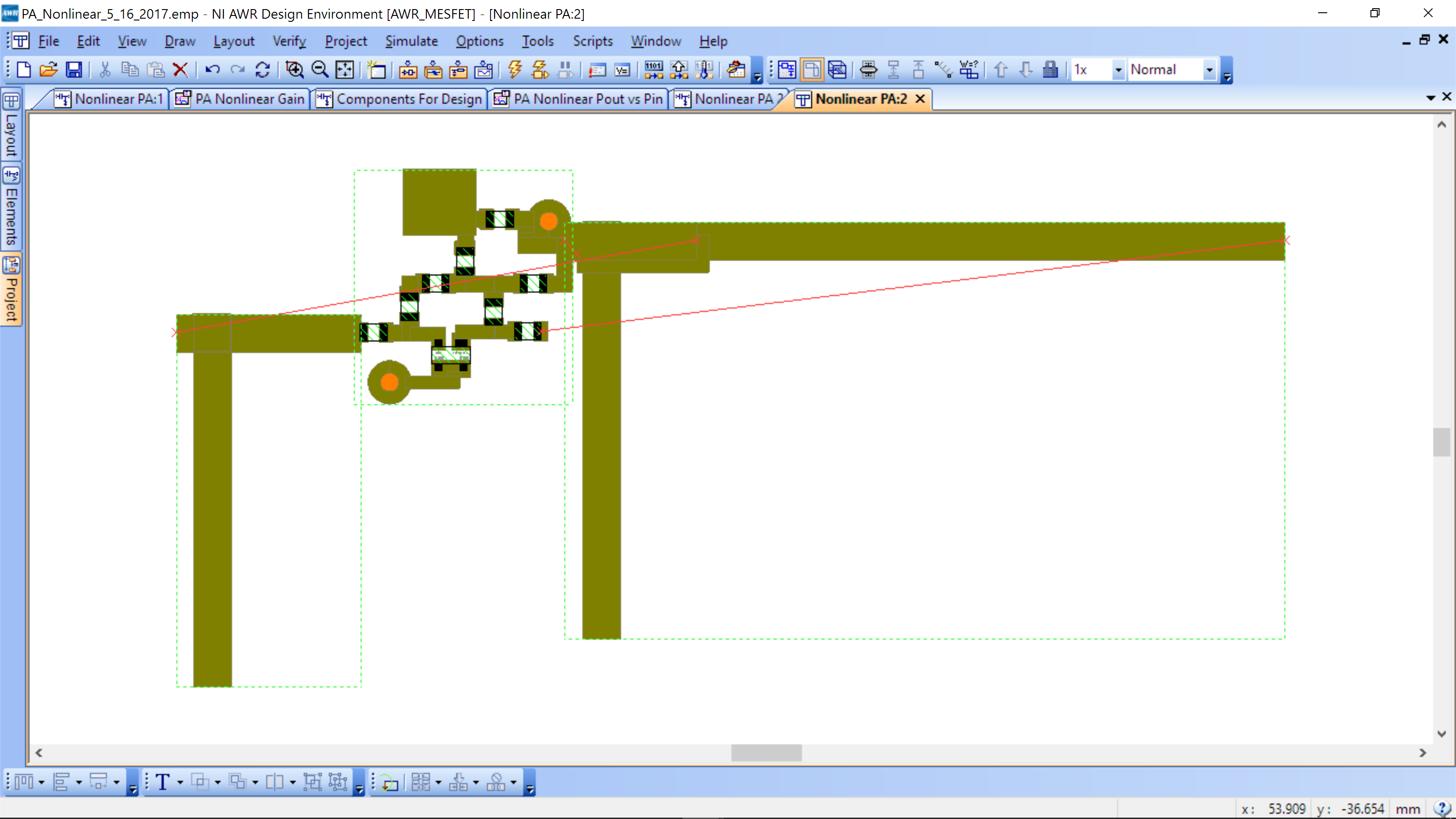
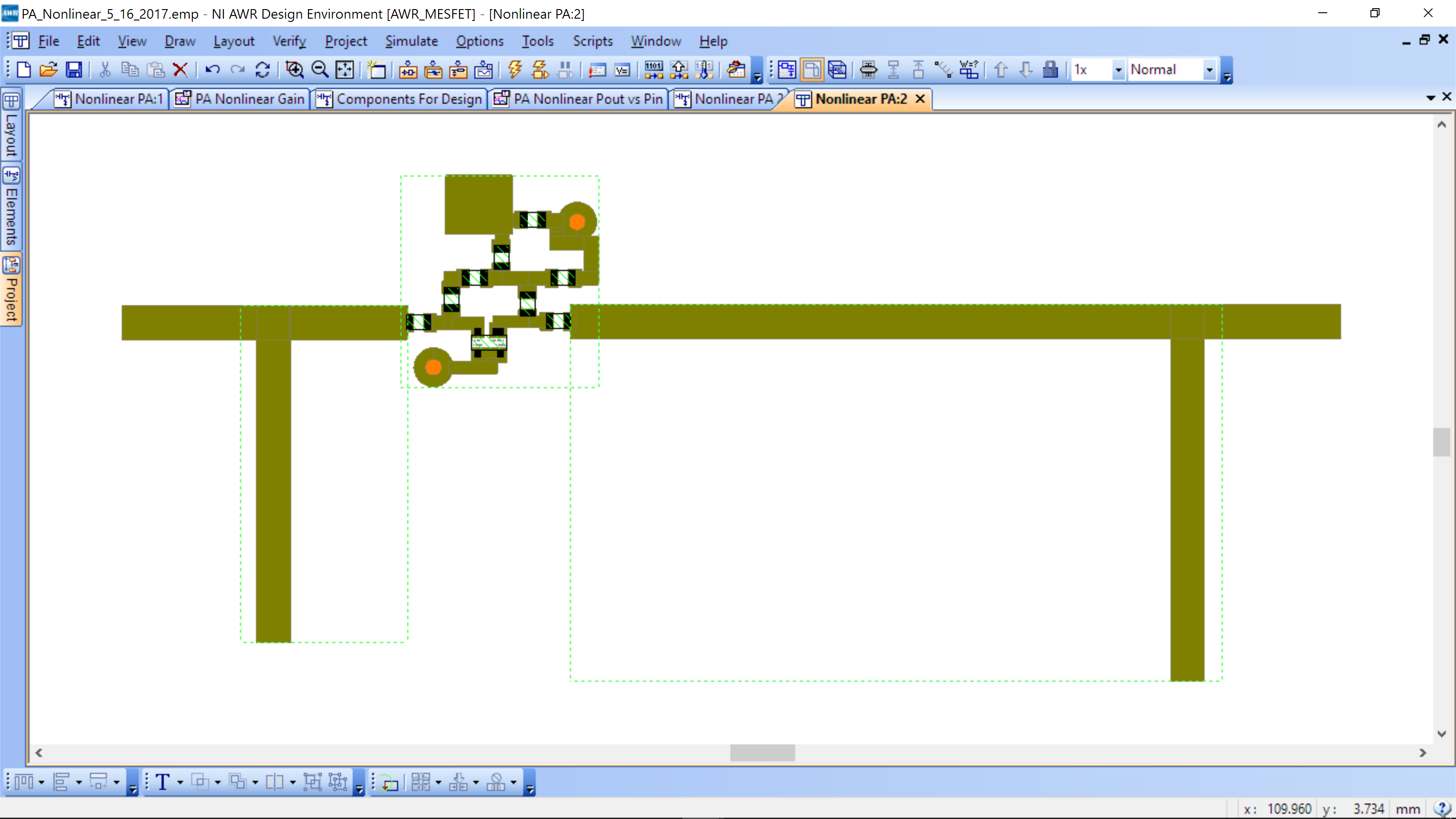
You will see that the BJT core is already laidout and so are the impedance synthesis network. To complete the layout, Ctrl+A, to select all, then Edit-> Snap Together. Since there is only one logical arrangement of the subcicuits, AWR is able to assemble the layout for you, see below.
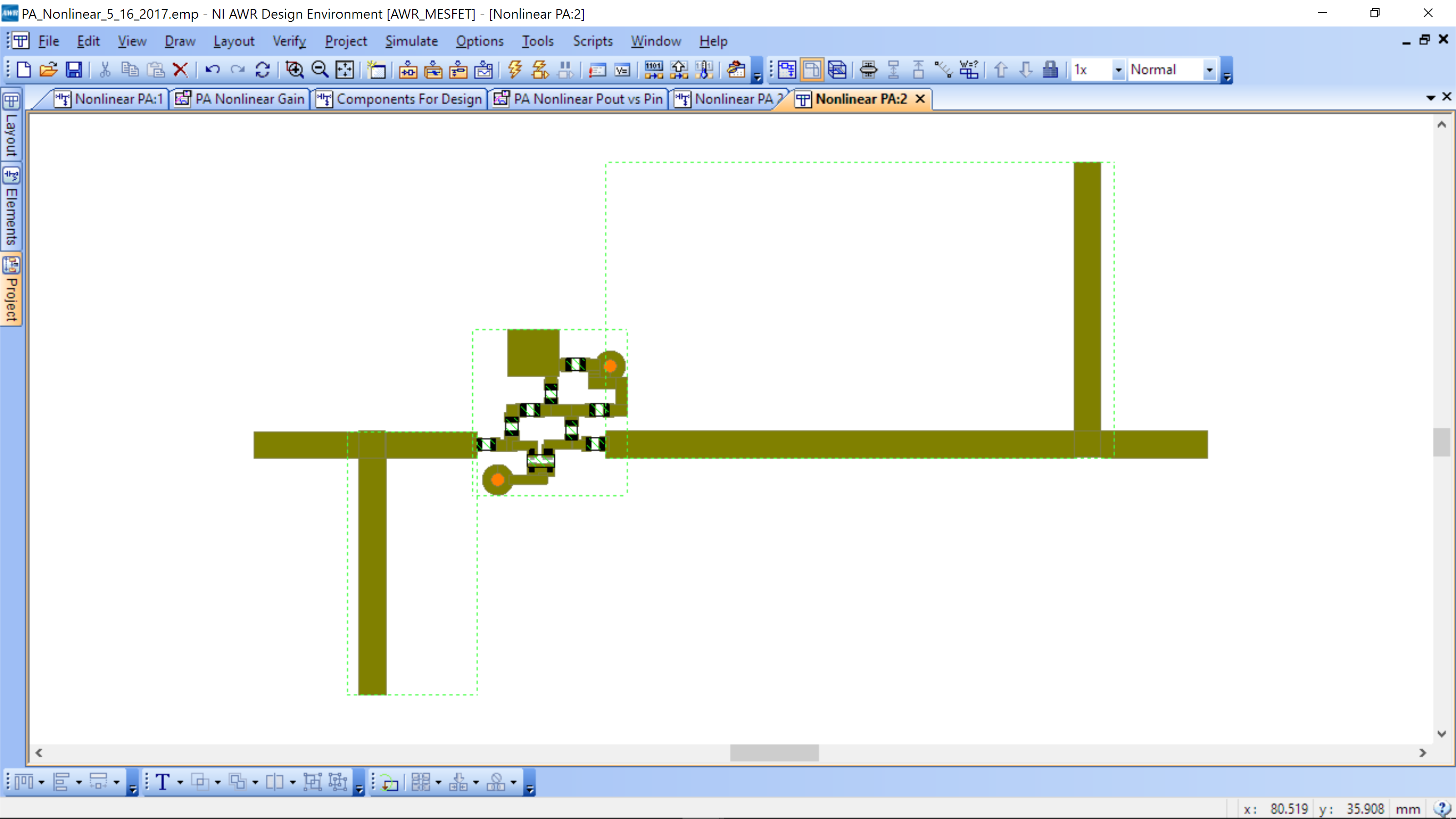
It is desirable to have both stubs point in the same direction (for space savings). You can flip the output impedance synthesis network and use the Snap Together sequence and you will have your final layout.
Optional – Meandering transmission lines (2D Cutter only, not foil method)
To fit on some PCBs you may need/want to “meander” the transmission lines with lengths L1 and L2. In the easy-to-build format of the workshop, we provide PCBs that are large enough to not require meandering and thus save significant time.
We will leave the transmission line of length L3=10mm straight.
Next we will replace the MLIN model for the two transmission lines L1 and L3 by MTRACE2. You can do this by just changing the name of the component in Schematic view. You will notice that the layout view is not changed! There is a difference however. Below is the modified output synthesis network, where we have masked out the design values for L1 and L2. Note that L2 has been split into MTRACE@ and MLEF. This is because the open stub does not have a meander option, so we leave the open end fixed at 10mm and replace the straight section of L2 with a meander section (equivalent microstrips, just one is easily shaped). Remember to subtract 10 mm form L2 length, as the final length will be L2+10 mm, which is the MTRACE2 plus the MLEF as shown below.
Go to the layout. Now double click on the line, three handles appear at the beginning, middle and end of the line. Double click again on the handle which is at the end where the arrow/triangle is and you will notice that your cursor changes to a drawing path (see figure (b) below). You can now draw a path, for example to meander the line (see figure (c) below). Once you are happy with the shape you want the line to look like double click and the line will be re-drawn according to your path. (see figure (d) below)

Notice that by doing this meandering the length of the line has not changed! This means the software will adjust the drawing in X and Y direction so that the total length remains constant – this is because of our use of the equation for “L1” and not the number in the L parameter of MTRACE2. This also means if the path you draw is longer than L1 of the MTRACE2 you specify in Schematic, the meandering shorten the line to the defined length. Also note that even though you changed the shape of the line in Layout the symbol in the Schematic is still one straight line. Once the line is meandered, you can adjust the spacing and extension by double clicking on it and moving the handles.
An example meander is shown below. Note that it is much shorter than the standard line. The left end is the 10 mm transmission line that connects to the SMA and the right side connects to the PA.
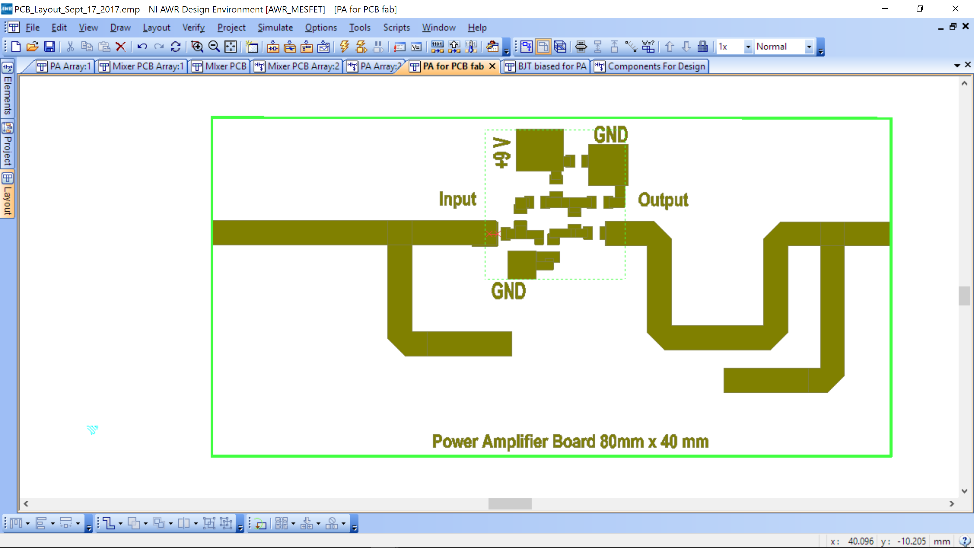
Meander both the input and output. The board outline (size) is 80 mmx 40 mm. Your amplifier and transformation network needs to fit inside of the board. Here is an example of the layout with impedance networks. The board layout is contained in the template as part of the BJT-biased-for-PA layout.
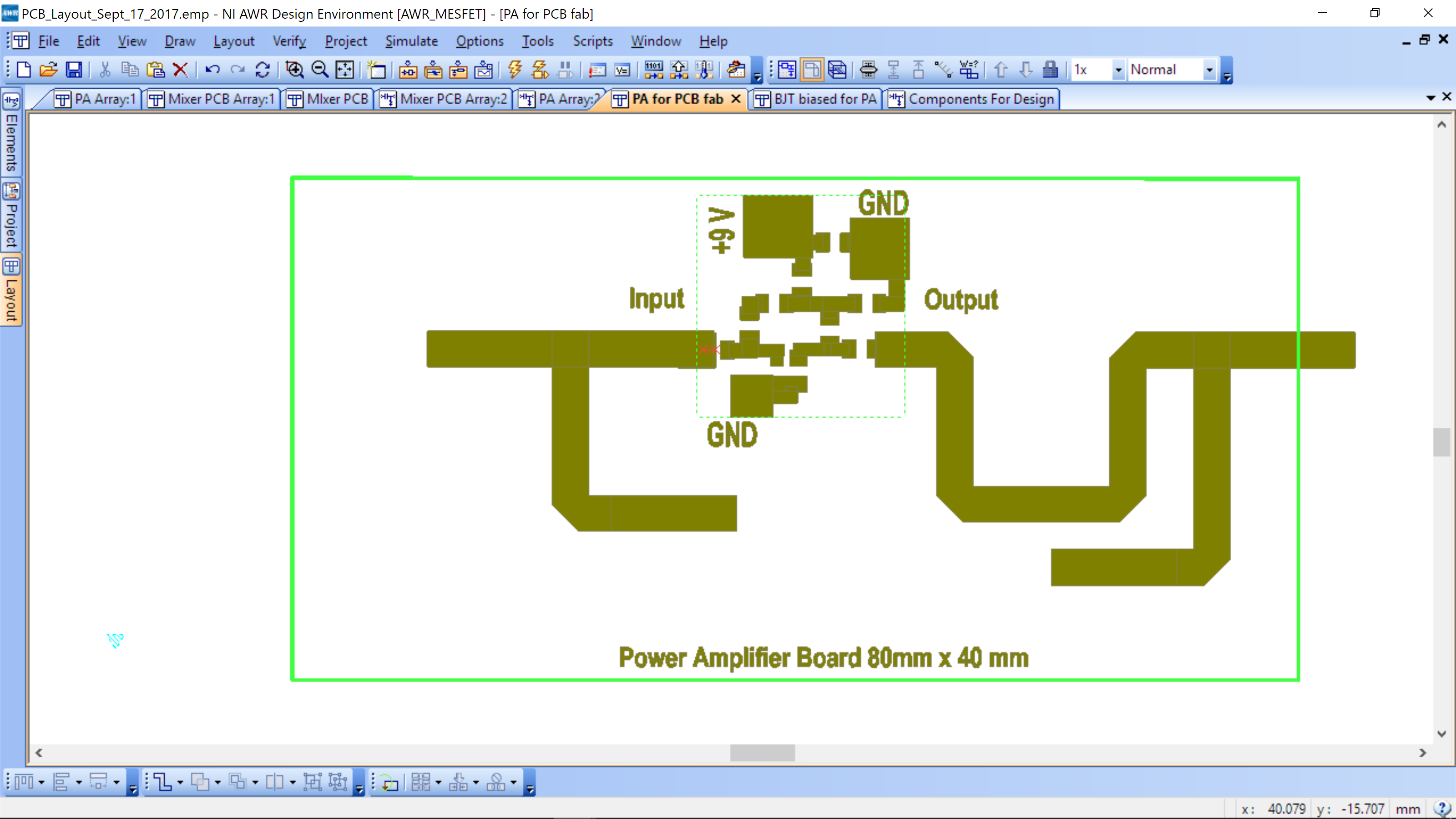
Note that the output is over the right edge and the left is not connected to the edge. You can simply add/remove to the 10 mm SMA feed transmission lines (L3) to match the board outline. This can be done manually in layout or you can change the length of each SMA feedline in schematic and then adjust in layout.
Assembly
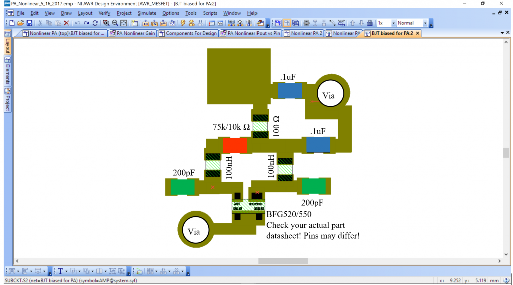
The layout with components values is shown below. You can find the components from the color-coded sheet in your kit. Note there is a unique identified for each component, which includes a combination of: Number of components in kit, package style, number of pins, shape of pins, and finally color on packaging.
The assembly of the ports is easy, just solder on an SMA connector. For the amplifier core, the following will assist assembly.
Note the 75k is for the LNA. a 10k resistor is used for the PA.
Also, check the specific layout of your PA board and your chosen transistor. Pad layout and pins may differ from image below. Use the schematic to see which way your transistor goes on the board.