
Bits to Waves Overview
“The NCSU Bits-2-Waves QAM Radio”
David S. Ricketts ()
North Carolina State University. Raleigh, North Carolina, United States of America.
Radio System Design and Fabrication of a Modern Digital Radio (16 QAM) you can Design and Build at Home
David S. Ricketts
North Carolina State University, Raleigh NC
In the winter of 1894, Guglielmo Marconi called his mother up to the attic where he had been tinkering with a new device called a “coherer” which could sense electronic signals forming a spark. He showed her how he could ring a bell from a few meters away with an artificial lightning bolt – a spark gap, just like Hertz had made before him. The era of wireless communication was born.
Imagine the late nights of Marconi working in his makeshift laboratory in the attic of his parents’ house, creating his device out of copper wire and ribbon, glass jars, iron filings, and a few rough tools. Marconi had the ability to build something and test it in a few hours—to go from the idea in his head to a prototype in his hands in perhaps only a day.
In today’s era of simulation and analysis, microprocessors, digital ASICs, and digital signal processing, it seems a far-fetched idea that a person could conceive of a modern radio and build it with their own hands as Marconi had done with his first radio, let alone do it all in one day. However, in this article, we present a project aimed at doing just that – one which brings the concepts of modern digital communications and radios into a form that you can design, build, and test in as little as a day.
Bits2waves [1] is an experiential program that introduces microwave engineers and enthusiasts to a modern Quadrature Amplitude Modulated (QAM) radio and takes them step-by-step through the design, simulation, layout, fabrication, and final testing of the key pieces of today’s radios.
Digital Radios
Almost all information is stored and processed in the digital domain – music, movies, radar images, etc. The airwaves, however, have remained analog. The digital radio is a modulator and demodulator (modem) that transmits ‘information’ through a convenient carrier signal. One takes for granted that radios use electromagnetic waves from 10 Hz to 300 GHz as the carrier; however, communication is not dependent on the carrier, it only uses the carrier as a means to transmit information. Beyond electromagnetic waves, light and sound waves are two other carriers that have been used for communication.
Claude Shannon was one of the pioneers to look at ‘information’ in an abstract sense, in particular in the context of communication. His theorem tells us the theoretical relationship between the maximum information that can be transmitted for a given channel bandwidth and signal-to-noise ratio (SNR). Significantly, his theorem does not depend on how the radio is built, but rather is determined by statistics and information theory. The proof of his theory is complex, but the results are simple and profound. The maximum capacity of a communication system is [2,3]:
C is the capacity or data rate, BW is the bandwidth, and Psig and Pnoise are the signal and noise power, respectively, whose ratio can be expressed as the signal-to-noise ratio, or SNR. This simple equation tells us not only what our maximum data rate could be, but also that the two relevant design parameters are BW and SNR, two concepts which are easy to relate to a radio system design.
The encoding of information onto a carrier for digital data is done by quantizing an analog parameter and using each quantized value to represent a specific digital sequence. For example, the amplitude of the carrier could be split into four levels—0, 0.5, 1 and 1.5 V—then each voltage could be assigned to a digital code. Since there are four levels, two bits can be used: 00 🡪 0V, 01 🡪 0.5, 10 🡪1V, and 11 🡪 1.5V. The sequence does not have to be monotonic, one could arrange the digital bits to levels in any manner – all that matters is that there are four values and four unique digital sequences. This idea can be extended as well, such that for M analog values (e.g., voltage levels), one can map 2k bits to them: M=2k.
| Bit | Symbol |
| 000 | +7 |
| 001 | +5 |
| 010 | +3 |
| 011 | +1 |
| 100 | -1 |
| 101 | -3 |
| 110 | -5 |
| 111 | -7 |
| k=3 | M=8 |
| Bit | Symbol |
| 0 | -1 |
| 1 | 1 |
| k=1 | M=2 |
| Bit | Symbol |
| 00 | +3 |
| 01 | +1 |
| 10 | -1 |
| 11 | -3 |
| k=2 | M=4 |
How are these different values made? On a propagating wave, one can vary the amplitude, phase, and frequency. While M could be made from any combination of these three variables, most systems use amplitude and phase because changing frequency, especially over significant ranges, can cause bandwidth and hardware challenges. Figure 1(a) shows a simple modulation if M=4, where only the phase is changed. We can, of course, vary both amplitude and phase, and create what is known as a constellation. The frequency of the carrier is assumed and not shown. Figure 1(b) shows M=4, where amplitude and phase are modulated. The phase is shown by the rotation around the x-axis. The x-axis can be thought of as cosine and the y-axis as sine, which of course are the same signal just 90° out of phase relative to each other..
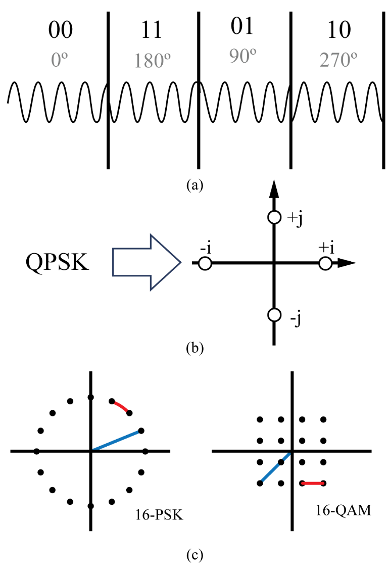 |
| Figure 1: (a) A quadrature phase shift key (QPSK) signal in the time domain. Each symbol is Tp seconds long. (b) A constellation diagram of a QPSK signal. (c) A 16-PSK and 16-QAM signal. The QAM uses both amplitude and phase (or quadrature amplitude) modulation to produce a given inter-symbol spacing, aka SNR, with less peak power than a PSK constellation. The inter-symbol spacing is the same in both QAM and PSK constellations, notated by the red line. The peak power, shown by the length of the blue line, is higher for PSK for a given inter-symbol spacing (length of the red). |
Each point is called a symbol. Figure 1(c) shows M=16 values. The first is called a Phase-Shift-Key (PSK) and has a constant amplitude and 16 different phases, 16-PSK. The second, 16-QAM, has varying amplitude and phases for 16 points. An easier way to understand this constellation is to consider creating the amplitude and phase from two orthogonal components, in-phase (I) and an out-of-phase (Q) signal. These are simply sine and cosine, or carrier and a 90-degree phase-shifted carrier. This is also how such constellations are generated in hardware. The representation with quadrature signals leads to the name Quadrature Amplitude Modulation (QAM), or 16-QAM in this example [2,3]. In viewing the constellation in I and Q, one can see that it has 4 amplitude levels and Q has 4 amplitude levels, which leads to 16 symbols in the constellation. An arbitrary number of symbols can be generated in a constellation. Practical systems have gone as high as 4096 symbols. The constraint is shown by the blue (maximum amplitude) and red (inter-symbol spacing) lines. The SNR is dependent on the spacing between symbols or points, as a noise constellation point needs to not interfere with its neighboring constellation points. In order to add more points with the same SNR, the constellation must get larger, and thus the peak power higher. QAM is preferred to PSK since for a given inter-symbol spacing (red line), the peak power (blue line) is shorter (1.6 dB less peak power).
Pulse Shaping
Figure 2 shows the time domain waveforms of a BASK (Binary Amplitude Shift Key). Unlike analog modulation, in digital communications, each symbol is valid for a time period of T, such that data is quantized in amplitude, phase, and time. The repetition rate of the symbol will be key to understanding the data rate and associated signal bandwidth.
The signal changes every T seconds from one state to the other. Let us look at just this change in a variable (could be amplitude or phase). The digital information appears as a stream of pulses, with a minimum pulse width of T. Consider just the minimum pulse and its Fourier transform, Fig. 2.
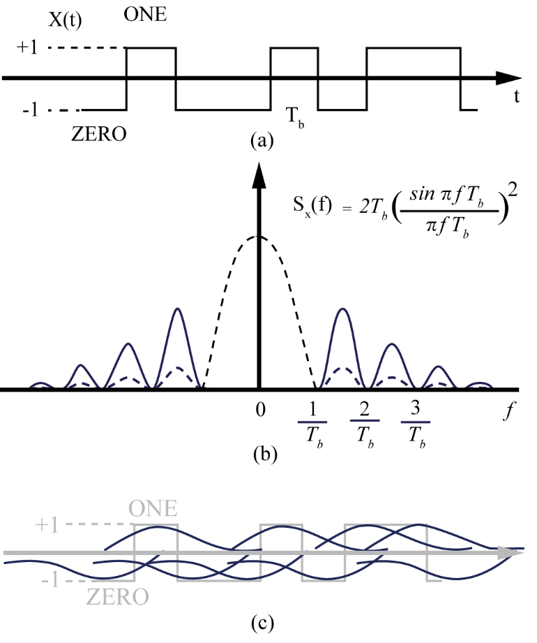 |
| Figure 2: (a) Typical digital signal to transmit. (b) Magnitude of power spectrum of a square pulse – note infinite bandwidth. Dashed line shows portion of waveform after a low pass filter (qualitative) (c) Square pulses are “smeared” by low pass filter. Value at any point is dependent on what signal came before. This is inter-symbol interference (ISI). |
In theory, its bandwidth is infinite. International standards strictly restrict the transmission bandwidth, thusprohibiting this simple approach of a sharp transition in symbols. A simple solution would be to filter the signal such that the bandwidth falls in the licensed band. In the frequency domain, this would work well (shown in Fig. 2b). In the time domain, however, a low pass filter “smears” digital pulses from one period to the next (shown in Fig. 2c). This “smearing” causes Inter-symbol Interference or ISI [2,3]. The voltage during period T1 is affected by whether or not there was a 1 or 0 in the previous pulse. ISI creates a significant problem and prohibits this simple bandwidth limitation approach.
Luckily, Harry Nyquist came up with a clever solution. ISI is only a problem because a pulse in the T1 period may affect future pulses (T2,3,4,…). What would happen if ISI occurred but, at one point in every succeeding pulse, it did not affect the value? This is done with a Nyquist pulse, which is the shape of a sync function. Not surprisingly, such a pulse has a square frequency spectrum (dual of the digital pulse in the time domain), which is ideal for band limited communication. Fig. 3 shows the Nyquist pulse and a series of Nyquist pulses. At the sampling time, all of the influence of other pulses is zero, as they are at a zero crossing. The only pulse that has a non-zero value is the pulse of that time period, T. The results is that the pulses do interfere with one another, but not at the sampling instant. The result is a band-limited signal without interference.
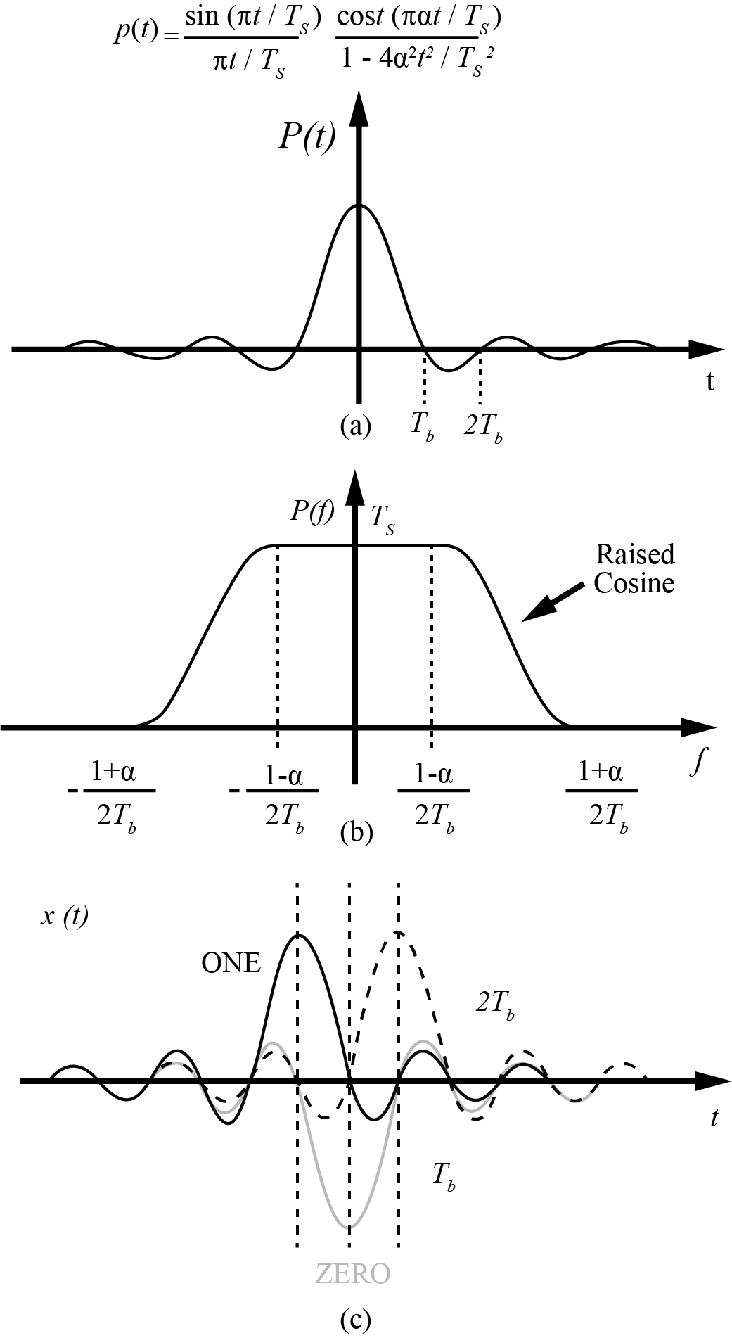 |
| Figure 3: (a) A Nyquist pulse in the time domain. Note it extends in negative and positive direction for infinity. (b) Raised cosine filter to create the Nyquist pulse (α = .35). (c) Series of Nyquist pulses. Note at every peak (sampling time) all pulses except the target pulse are at a zero crossing. |
The only challenge with the Nyquist pulse approach is generating the pulse. Instead of a perfect box in the frequency domain, a raised-cosine filter is used. It is an artificially-created filter profile which has a cosine shape leading and falling edge in the frequency domain, Fig. 3(b). The sharpness of the transition is determined by a parameter α. For an α of 0, it is a perfect square (and impossible to realize). Many systems use an α=.35 as a compromise between implementation complexity (lower α) and signal bandwidth (wider with larger α). The actual filter, owing to the need to have the time domain signal start before the pulse, is done in digital signal processing (DSP), such that the signals sent to the I and Q channels of the radio are already filtered (or shaped) in the digital domain and then converted to the analog domain by a digital-to-analog converter (DAC). The DAC usually has 4-8 samples per period, T, to create the appropriate pulse shape. In the time domain, this filtering is called pulse shaping, as it shapes the pulse from square to a sync shape.
Radio Architecture
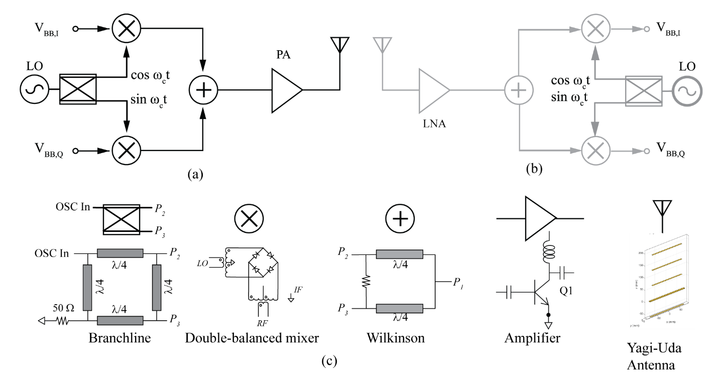 |
| Figure 4: (a) Quadrature architecture transmitter. (b) Receiver architecture (greyed since the receiver is not part of this article). (c) Circuit diagram for each of the five components built. An external oscillator is used. The branchline coupler is used to generate the cosine and sine local oscillators from the external oscillator. |
The radio architecture is shown in Fig. 4 [2,3,4]. The I and Q inputs come from the DAC of the digital baseband. Baseband refers to the information signal, as opposed to the RF signal, which is the carrier modulated with the information. The DSP has separated the signal into I and Q and also shaped them for limited bandwidth.
The baseband signal I and Q are just two signals; the radio establishes I and Q orthogonality (90-degree phase shift) by multiplying the I by a cosine at the RF frequency and the Q by a sine at the RF frequency (or vice versa). This also upconverts the baseband signal to RF using the basic trig identity:
The multiplication is done by a mixer. The cosine and sine RF signals are generated by a local oscillator (LO), whose output is split into two paths, with a 90-degree phase shift between them. The I and Q signals are then simply added together. Note, since they are orthogonal, adding them together does not cause any interference. In the receiver, the sum of I and Q will again be multiplied by cosine and sine, and the I and Q signals will be recovered.
The combined I and Q at the carrier RF is then amplified by a power amplifier. The power amplifier is simply an amplifier that has been designed for maximum output power and efficiency, usually at the expense of linearity. The signal is then transmitted through the antenna.
The receiver follows the same architecture, Fig. 4b, except after the antenna, a low-noise amplifier (LNA) is used. The LNA is simply an amplifier that is designed for lowest noise, usually at the expense of power and efficiency. The signal is split, and then multiplied by an I and Q RF carrier, generated by the same type of LO, and the signals are sent to an analog-to-digital converter in the digital receiver. Note that the correct reception of the transmitted signal requires the LO of the receiver to have phase and frequency locked to the transmitter. This is called a coherent receiver. The phase frequency locking is generally done by a phase-locked-loop in the receiver that synchronizes the LO with the incoming RF signal. This is not discussed in this article. Full testing of the radio can be done by simply using the same LO for transmitter and receiver, which is done in the live workshops.
The radio circuits to build consist of: 950 MHz oscillator, Wilkinson combiner/splitter (combines/separates signals with no phase shift), branchline coupler (splits the signal and generates 90-degree phase shifted signals), power amplifier, and antenna.
Wilkinson Combiner
The Wilkinson combiner is a three-port network that combines or splits a signal into two equal parts [2]. The signals are combined/split in-phase, such that the relative phase is not changed (the absolute phase will change). The Wilkinson combiner, Fig. 5, consists of two quarter wavelength transmission lines and one balance resistor, R1, which is shown split into two series resistors, R1a and R1b, which will be named and used for analysis only.
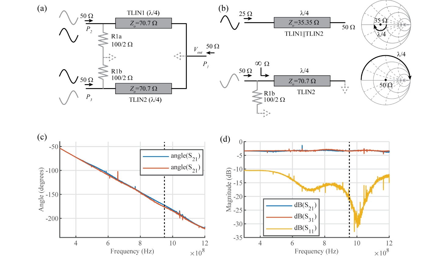 |
| Figure 5: (a) Transmission line model for even and odd modes. (b) Analysis of λ/4 sections for even and odd mode. (c) Phase difference, 4 degrees at 950 MHz (dashed line). (d) S11(-30 dB) and S21/31 (P2=-3.2 dB) and (P3=-3.3 dB) of the two input ports. |
The figure shows the actual components as solid lines, and two virtual grounds as dashed lines (not actual connection in the physical circuit). The operation of the Wilkinson can be understood by analyzing the even and odd modes of the input. This is the same as analyzing a signal as common mode and differential mode. Any signal can be split into an even/odd or common/differential mode. Doing so makes the analysis easier, as superposition can be used to examine each mode separately then add the two for the final answer.
For the even mode (black lines), the two inputs are in phase and therefore no current flows in the balance resistor R1, and it can be ignored. The two transmission lines are then simply in parallel, and the powers in each path are combined/split for even mode. The combined transmission line is equivalent to a 35.35 Ω transmission line. The λ/4 length of the transmission line will convert the 50 Ω RF output to 25 Ω at the input, which will then impedance match with the two inputs, which when paralleled have an equivlant resistance of 25 Ω. The impedance transformation can be graphically understood from Fig. 5b. A λ/4 transmission line rotates an impedance in the Smith chart 180° around a circle centered at the Zo of the transmission line (50 Ω →25 Ω).
For the odd mode (grey lines), the inputs are differential, and the center point of the balance resistor and output can be considered virtual grounds, separating the two paths from one another (isolated). The λ/4 transmission line transforms a short (gnd) to an open; this is simply a transformation around the outside of the Smith chart.
Thus the Wilkinson combiner combines/splits even modes and isolates odd modes, while providing 50 Ω impedance matching at all nodes.
Branchline Coupler
The branchline coupler is used to generate quadrature signals for our QAM radio. The Branchline coupler is a signal divider that can separate an incoming signal into two signals of equal power, but 90-degree phase-shifted. [2]. It consists of 4 ports: Input (P1), Output 1 (P2) and Output 2 (P3). The fourth port (P4) is terminated at 50 ohms for the signal splitter and is isolated from the input. The Branchline uses four λ/4 transmission lines with two characteristic impedances: Zo and Zo/√2.
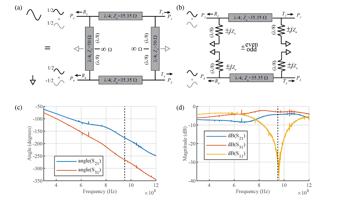 |
| Figure 6: (a) Transmission line model for even (black) and odd (grey) modes. (b) λ/8 section converted to impedance. Both even and odd modes have an impedance as shown by the resistor. The difference is in the value, wich is the same magnitude, but differs in sign (even +, odd -). (c) Phase difference, 89.4 degrees at 950 MHz (dashed line). (d) S11 (R1=-30 dB) and S21 =-3.16 dB and S31=-4.39 dB. The magnitude imbalance is due to the different path loss between P1 and P2 and P3. |
As with the Wilkinson, even/odd mode analysis will be used. Figure 6 shows the even/odd mode input to the coupler; note that the single-ended input (how the circuit is used in the radio) can be decomposed into two half-amplitude even modes and odd modes. For the even mode, like with the Wilkinson, current does not flow through the connecting transmission line. This does not mean there are not modes inside the transmission line, but rather that no net current flows. This is equivalent to their being a virtual “open” at the midpoint (λ/8). Likewise, for the odd mode, the midpoint is a “short.” The circuit can then be split into a top and bottom half.
The λ/8 transmission lines can be replaced by an equivalent impedance to ground using the standard input impedance equation for a terminated transmission line:
Noting that for λ/8, βl=π/4 and tan(π/4)=1, thus the impedance and admittance looking into the (λ/8 transmission lines are simply (even -,+; odd +,-):
The reflections, R1 and R4, and the transmissions, T2 and T3, are then calculated by finding the ABCD matrices for each component (recall ABCD allows oneto simply multiply components that are physically in series), then using the matrices to find the reflection and transmission of the coupler. Using standard textbook equations for the two shunt impedances (jYo) and λ/4 transmission line, ABCD matrix for the even and odd modes are:
Once again using tables from a textbook [2], the reflection (Γ ) and transmission (T) of half circuits can be found (the upper sign is even, the lower sign is odd):
The final reflections and transmissions can be calculated from the above and Figure 6:
where the minus sign on P3 and P4 result from the odd mode input that is inverted from the even on the lower branch. P1 is matched (R1 is zero) and P4 is isolated.The power is split between P2 and P3 due to the , with a 90-degree phase shift due to the j term, which is exactly our desired result for the LO quadrature generation.
Double Balanced Mixer
A mixer multiplies two input signals to provide an output signal. The inputs can be IF and LO (to obtain the RF signal), or RF and LO (to obtain the IF signal). Multiplication is done through nonlinearity of a device, typically a diode. One easy way to understand this is to consider the Taylor expansion of the exponential I-V characteristics of a diode.
By applying the two signals to multiply to the input, e.g.
The squared term of the Taylor series will create a cross product term, , , which leads to the desired up/down conversion of: . All that is left to do is to filter out the unwanted frequencies from the squared term and the other terms of the Taylor series.
Filtering out the different frequencies, in particular, the LO, can be achieved by choice of architecture. Balanced mixers reduce or remove the LO through differential signals. In this radio, a double balanced mixer will be used, which is a common, high-quality passive mixer. It is a double balanced mixer because both the LO and RF are balanced (differential) at the diode bridge.
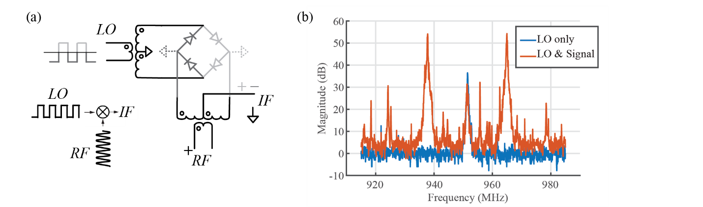 |
| Figure 7: (a) Mixer operation. Input LO turns the diode bridge into a switch, creating a virtual ground each half-cycle. This alternates the polarity of the RF signal on the IF port, which is equivalent to multiplying the RF by a square wave, which contains the LO as its first harmonic. (b) Mixer experimental results. 20 dB IF-LO separation. Overall conversion loss is – 10 dB (not shown). |
To analyze the double balanced mixer we will consider the operation for a large LO only, and treat the diodes as switches [3,5]. Figure 7a shows a double balanced mixer, where both the LO and RF are balanced, or differential. This is achieved with a Balun (derived from balanced-unbalanced), which is simply a single ended (unbalanced) to differential (balanced) transformer.
Consider two phases of the LO. When the LO is positive, or light grey, the two diodes on the right are forward-biased and form a virtual ground at the node shown. It is a virtual ground as it can sink and source current through either diode. The left side of the diode bridge is off. With this virtual ground, the input RF signal is transferred to the IF output with the same polarity. When the LO is negative, or dark gray, the two diodes on the left are forward-biased, and a virtual ground is made at the node shown. The RF signal is then transferred to the IF output with the opposite polarity due to the dot convention shown. The result is that the RF signal alternates polarity from same to opposite, every half cycle of the LO.
The result is equivalent to multiplying the RF signal by a square wave, as shown in the figure. The multiplication of the RF and LO signals can be seen by taking the Fourier series of the square wave and multiplying it by the RF signal In the example only the difference signal is shown; there would, of course, be a sum signal of the RF and LO signals. Most notable is that there is no LO term, which typically causes interference as it usually has power similar to or greater than the IF signal. In this simple design, there is no impedance matching at the RF and LO nodes.
Power Amplifier
Power amplifiers are amplifiers that optimize output power and efficiency, rather than linearity (although linearity isn’t specifically excluded, it’s just not one of the optimization metrics).
In this radio, a Class-AB amplifier will be used, which is simply an amplifier operated between Class A and Class B (to be explained shortly) [6]. Figure 8a shows the basic operation of the amplifier. When biased so that the transistor is always ON, the amplifier is said to be Class A. This is a simple linear amplifier with maximum efficiency of 50%. When the signal is large enough (or the bias low enough), the transistor turns off for a portion of the RF cycle. When it turns off for one-half the time, the amplifier is said to be Class-B. This introduction of nonlinearity (clipping) leads to higher efficiency. At the same time, this approach creates harmonics of the fundamental due to the nonlinearity. The harmonics can be removed by filters that terminate or shunt the harmonic currents using transmission line circuits or lumped filters.
The higher efficiency can be seen through the overlap of the voltage and current waveforms. In the Class-A there is always a non-zero current, and thus there is always an overlap of collector voltage and current, resulting in low efficiency (maximum 50%). In the Class-B, when the voltage is high, the current is zero, so, in theory, there is no loss. The result is a much higher power efficiency as will be shown shortly.
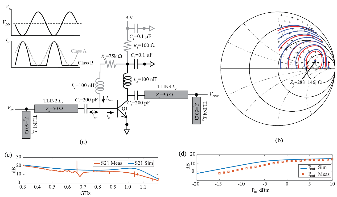 |
| Figure 8: (a) Schematic of power amplifier with Class A and B waveforms in upper left inset.
Gray is DC bias, black is RF path. Input and output impedances are synthesized by a transmission line network, whose lengths are adjusted in simulation to provide the desired impedance at the input and output of the PA. (b) Loadpull results showing optimal load impedance, ZL for a NXP BFG520 BJT transistor. Red is power output and blue is efficiency. (c) Measured results of PA gain: 12.96 dB at 950 MHz. Measured output power versus input power. Psat is 14.3 dBm. |
This “clipping” of the collector current will generate harmonics, which are filtered out by the LC tank at the output.
The efficiency can be calculated by counting the RF and DC terms in the Fourier series of the “clipped” current. The resulting efficiency is:
This is a significant increase in efficiency over a Class-A; however, the output is no longer a linear relationship to the input. This is often the tradeoff in power amplifiers.
The output power of the amplifier is determined by its bias condition (collector current for the BJT) and the output impedance. Unlike linear amplifiers, whose output power is maximized when the load is a complex conjugate of the amplifier output, nonlinear power amplifiers often exhibit maximum power and efficiency with non-conjugate matched loads. For large signals, it is not the output impedance that is important but rather the load impedance that matters [6,7]. Output power is maximized when the maximum current is extracted from the transistor amplifier, and efficiency is maximized when the loss in the transistor is minimized. Both are dependent on the shape of the collector waveform, which is dependent on the bias as well as the load impedance. Generally, the ideal load for efficiency and power is not the same [7], although they are very close for this particular design.
A simple technique is available to analyze the maximum output power and efficiency, called load-pull. The amplifier is operated in its target operation mode, e.g., Class-B at maximum amplitude, and a complex load modulated at the output. The power and efficiency are measured (simulated) for each complex load and plotted on a Smith chart. When plotting the loads that produce the same output power, one will see that they form a circle, Fig. 8b. The load-pull produces a series of circles at each power, with higher powers generally achieved for a smaller variance in complex load.
Fig. 8b shows a load pull performed in simulation. The maximum power is achieved at the point 288+146j Ω. This is the target load to achieve maximum output power. To maximize input power, a simplified approach is used, where the PA is terminated with the target load found from load-pull. The small signal input impedance of the PA transistor base is then measured. For the input we adopt a small signal approach and use the complex-conjugate (maximum power transfer for small signal) as our target input network impedance. In our design, it is 18-11jΩ. It is possible to further optimize both the load and input impedances through iteration (using the small signal conjugate as the input instead of the 50 Ω load used in the original load pull) and other advanced techniques.
With the target load and source impedance found, an impedance-matching network is synthesized to impedance transform the 50 Ω RF source and load to the desired PA source and load impedances. There are numerous techniques for this transformation. To ease design and implementation, a simple topology was chosen and the lengths simply adjusted in simulation until the desired impedance match was obtained. Figure 8a shows the basic topology of an open transmission line stub of length L2,3 in parallel with a series transmission line of length L1,4. While one can certainly calculate the exact value for the transmission lines, it is simpler to use the optimization or “tuner” functionality found in most computer aided design (CAD) software. One can assign a nominal value (20 mm), then adjust the length until the 50 Ω ports are transformed to the desired input and output impedances. (Note: this is best done as a separate simulation. To do this, set up the transmission line network and terminate with two 50 Ω ports. Then adjust the lengths so that ZIN is your desired impedance, e.g., ZIN=ZL=288+146j Ω (Fig. 8b). Then add the network to the PA for final verification.)
The simulation and experimental results of the PA are shown in Fig. 8c and d. The small signal gain was comparable at low frequencies; however, it differed by several dB at 950 MHz. Given that the transistor was not modeled at RF, this discrepancy is small. The dip in measured S21 is due to a secondary resonance in the matching networks. Due to the lower gain, the Pout vs. Pin is shifted to the right but achieves almost the same output power of Psat=14.45 dBm and S21 of 13 dB.
Antenna – Yagi-Uda
While many antenna designs could be used with the radio, a Yagi-Uda directional antenna provides both high-gain as well as an interesting design. One can understand the basic operation of the Yagi-Uda by considering a ½ λ dipole antenna, Fig. 9. The charge on the antenna oscillates between each end of the dipole, creating an electric field that couples to free space and propagates outward on both sides of the dipole.
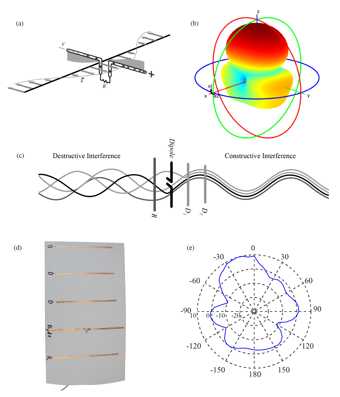 |
| Figure 9: (a) Electric fields generated by an alternating current in a dipole. (b) Calculation of the fields from a 3 director Yagi-Uda antenna at 950 MHz. (c) Operation of a Yagi-Uda antenna. (d) The fabricated Yagi-Uda antenna using 2.5 mm copper foil. (c) The measured results of the antenna with a 7.5 dB gain, slightly off center at 15 degrees. |
In an antenna, the directivity is characterized by the gain of the antenna. The gain is simply how much more power is transmitted (received) in a given direction than would be if the antenna transmitted in all directions (isotropic). For a ½ λ dipole antenna the maximum gain is 2.15 dBi (dB compared to an isotropic antenna), which has about 60 percent more power in the direction perpendicular to the antenna than an isotropic antenna. The dipole, Fig. 9a, radiates by stimulating an alternating voltage in each of the two sides, which couples to the air to create a propagating wave.
To increase the gain (directivity), the Yagi-Uda antenna does two things. First, it reflects the energy propagating away from our desired direction with a reflector. Second, it directs the waves so that they are aligned in the desired direction. This is done with one or more directors. The qualitative operation of the Yagi-Uda antenna can be understood by examining Fig. 9c. The goal of the reflector is to create a destructive wave going behind the antenna (to cancel the dipole radiation) and a constructive wave in the desired direction. The reflector is stimulated by the dipole and radiates a wave that is time-delayed by its distance from the dipole. In addition to phase shift due to the time-delay (distance), an additional phase shift can be introduced by shortening the reflector, similar to a resonator off resonance – its phase is shifted from the input. The directors operate in the same fashion; however, they are placed in front of the dipole and aid in constructive interference of the waves so that they are “focused” in the desired direction. The phase of the reflector/director is initially out of phase from the incoming wave but, due to the time shift and the phase shift by shortening the element, different phase shifts for the reverse and forward waves can be achieved. This can be seen qualitatively in that the directors are typically shorter than the dipole and reflector, to adjust the phase properly.
The design of the Yagi-Uda antenna can be done with simulation software. However, a very good experimental study was done in 1976 which provides basic design guidelines for antennas and can be found in Table 1. (p7) of [8]. In order to fit on a standard sheet of paper (A4), a length of 0.8 λ was chosen, or 25.3 cm (λ=31.56 cm at 950 MHz). The next parameter to choose is the conductor element in terms of λ. The design provided in Table 1 shows a ratio of 0.0085λ, yielding a wire diameter or 2.68 mm, which is very close to 10 AWG wire (2.58 mm).As a result, simple cut lengths of standard 10 AWG wire can be used for all elements. The reflector is given as 0.482λ and the directors, 1 through 3, as 0.428λ, 0.424λ, 0.428λ respectively. The spacing of all elements is 0.2λ. The dipole is nominally 0.5λ with a stand-alone input impedance of 73 +j 42.5 Ω. This input impedance can be adjusted by simply shortening the dipole and measuring the return loss, or by designing an impedance-matching network.
Figure 9d and 9e show our fabricated antenna, as well as the simulation and measurement results. To ease fabrication, 3 mm wide copper foil was used instead of 10 AWG wire. Experimental results showed that this produced as good results as wire and is much simpler to make. Tuning of the input was done by fabricating the dipole at about 0.6λ and then simply trimming with a knife until it matched well at 50 Ω.
QAM Transmitter
The components above were fabricated using a simple craft foil cutter and copper sheets with adhesive backing (also used for crafts) [9]. The layout was taken from NI/AWR Microwave Office and imported into the cutter software, which then cuts an outline of the copper traces in the copper foil. Any CAD software that can export a .dxf file would work. A quick transfer of the foil was applied to the bare side (no copper) of a single-sided FR4 PCB. The copper side for the FR4 provided the ground plane for all microstrip lines. The mixer and power amplifier core were pre-fabricated, owing to the lack of resolution of the cutter. The impedance-matching networks were all that were added to the PA. The antenna was made from copper foil strips, placed directly on cardboard or similar (mostly air) substrate.
Figure 10 shows a completed radio. This radio has been successfully fabricated by students in a single 8 hour day (or less) at European Microwave Week 2018 and the International Microwave Symposium 2018. A test 16 QAM constellation is applied to the I and Q IF inputs. The pulse-shaped signals are generated using a pseudo random number generator to generate an example digital signal, similar to Fig. 2a. This is then converted in to Nyquist pulses using a raised cosine filter (in matlab or other software program), Fig. 3b, with a sampling rate of 8 times the period of each symbol period (sampling is simply approximating the analog waveform with 8 discrete voltages per period). The sampled version of the waveforms are then saved as an .mp3 audio file. The input to the radio is from an mp3 player and a headphone cable, with the right stereo output connected to the I and the left stereo output connected to the Q. A sample .mp3 file is provided on the website for testing [1]. The receiver is a duplicate of this radio, minus an LNA (it was not needed for short distance). The received I and Q are sampled by the audio input of a laptop (once again using the right and left channels of a standard 3.5mm audio cable connected to the I and Q outputs of the receiver) using a standard Matlab/Python function. The audio input provides an easily accessible analog-to-digital converter to digitize the radio output. Once read, they were plotted using Matlab. The code for reading the laptop port and plotting are provided on the website [1]. Figure 10c shows the constellation sent to the transmitter. Figures 10d and 10e show the received signal without and with the PA, respectively. The transmit and receive antennas were placed next to one another with an estimated 15 dB of signal path loss.
The received constellation without a PA, Fig. 10d, is rotated due to the phase change as the signal propagates through the air. For example, a cosine will look like a sine if you are a distance of λ/4 away. The constellation rotates around its center as the signal propagates through the air, returing to the original orientation every integer wavelength away. The modern software receiver can simply rotate the entire constellation, reagardless of its received rotation, to its original “square” orientation (it is a simple mathematical rotation of the received data). The received signal using the PA is shown in Figure 10e. It is larger as expected and shows some distortion – the constellation is no longer a perfect square. These imperfections are caused by non-uniform gain in the I and Q paths as well as an imperfect 90° phase shift in the I and Q LO. Some of these are present in Fig. 10d without the PA. Additional distortion is caused by the PA saturating and not being able to completely form the end points of the constellation. The phase delay through the PA causes the rotation to be different than Fig. 10d, however this does not affect the reception of the constellation. The resulting error vector magnitude (EVM) was 2 percent, which was partially limited by the original signal from the DAQ. EVM is a measure of the average error from the actual constellation point and the ideal point [3]. It is related to non-idealities in the radio link as well as SNR.
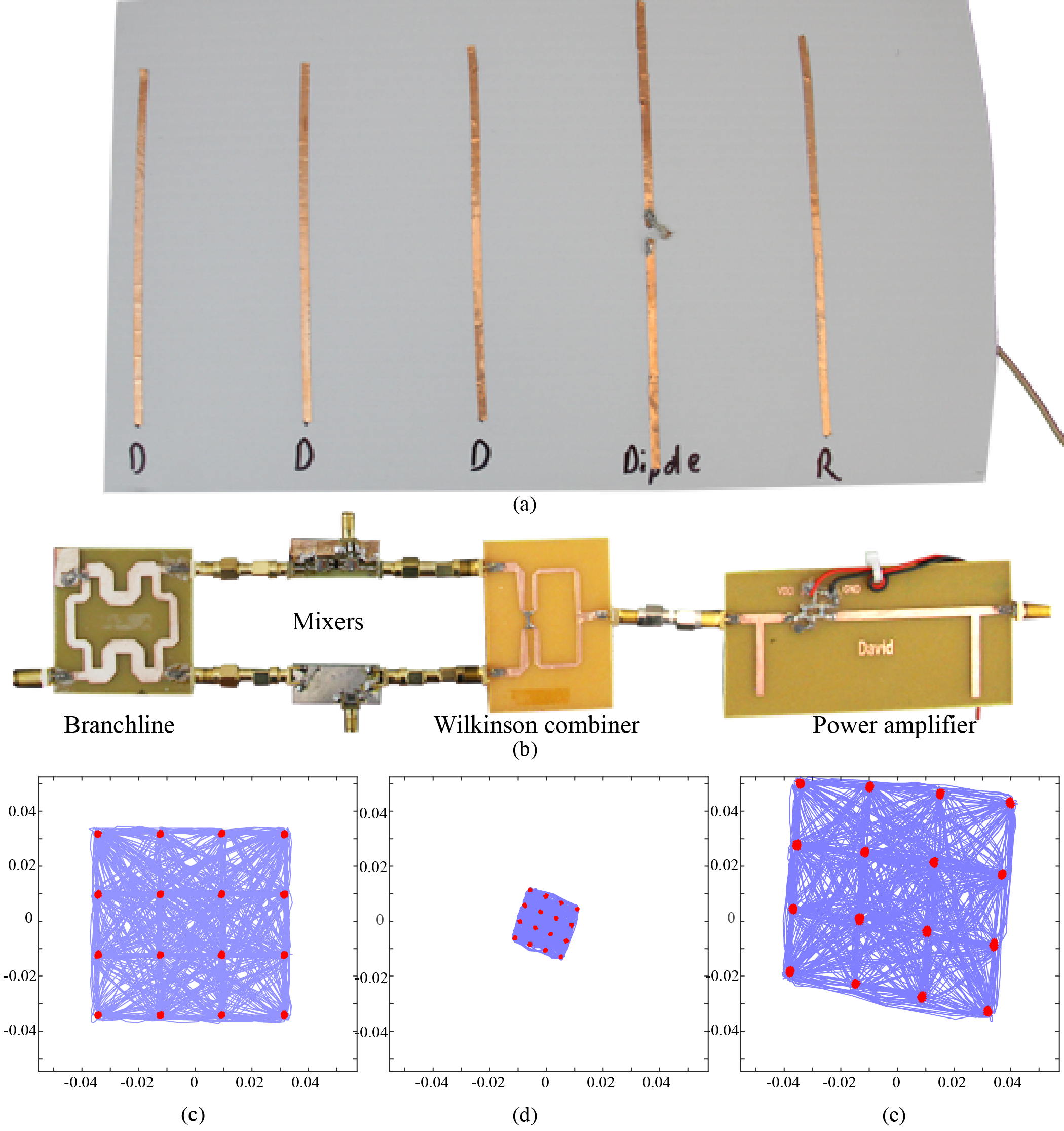 |
| Figure 10: (a) Yagi-Uda antenna. Dipole is marked, along with reflector (R) and 3 directors (D).
(b) QAM radio. (c) Input constellation to transmitter. (d) Received constellation without PA. (e) Received constellation with PA. EVM was 2%. |
Conclusion
In this article, we overviewed the history and development of digital radios and the associated microwave hardware. Through short tutorials, we showed an easy method for understanding and designing the basic components of a modern digital radio. Through simple fabrication using home craft cutters and simple circuit components, a radio was constructed that was able to transmit 16 QAM signals in high SNR. A complete step-by-step tutorial is available on www.rickettslab.org/bits2waves along with additional details on the parts list and fabrication.
[1] D. S. Ricketts, “Bits2Waves – Build a 16 QAM 950 MHz Radio,”. [Online].
Available: http:// www.rickettslab.org/bits2waves. [Accessed Jul. 1, 2019].
[2] Michael Steer, Microwave and RF Design, Scitech Publishing, 2013.
[3] Steven. W. Ellingson, Radio Systems Engineering, Cambridge Press, 2016.
[4] David M. Pozar, Microwave and RF Design of Wireless Systems, John Wiley & Sons, Inc. 2001.
[5] Jon B. Hagen, Radio-Frequency Electronics, Cambridge University Press, 1996.
[6] Steve Cripps, RF Power Amplifiers for Wireless Communications, Artech House Microwave Library.
[7] Guillermo Gonzalez, Microwave Transistor Amplifiers, Prentice Hall, 1997.
[8] Peter P. Viezbicke, “Yagi Antenna Design”, NBS Technical Note 688, December 1976
[9] D. S. Ricketts, “Bits2Waves – Build a 16 QAM 950 MHz Radio,”. [Online].
Available: http:// www.rickettslab.org/bits2waves/fabrication. [Accessed Jul. 1, 2019].