
Wilkinson Theory
3dB Wilkinson Power Divider
In this part of the workshop, you will design a 0.95GHz 3dB Wilkinson Power Divider circuit.
The Wilkinson Divider is used to both divide and combine signals, maintaining their phase. Unlike the branchline coupler, the Wilkinson will split a signal into two signals with 0 phase shift between them. The Wilkinson divider achieves excellent isolation through the use of quarter-wavelength transmission lines and a balance resistor between the inputs/outputs. The difficulty in realizing a Wilkinson divider is that balance resistor is a discrete element and much smaller than the transmission lines. To connect it between the two ports, the transmission lines need to be “bent” to almost touch so the connection to the resistor is short. At the same time the transmission lines need to be far away from one another so the two paths do not couple. As you will see shortly, the typical layout for a Wilkinson combiner looks a bit strange!
Theory of Operation
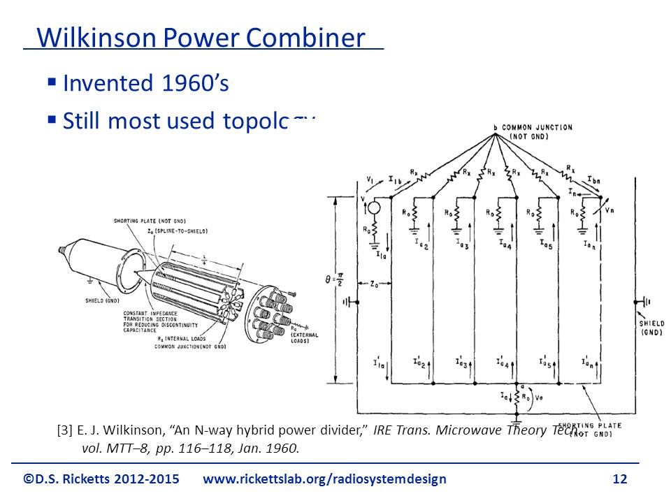
The solution to this problem is called a Wilkinson power combiner. It was invented in the nineteen sixties and is still the most used topology. He used transmission lines and put them in a radial configuration with the inputs, combining them to a single output as shown on the left side of the figure. Notice that each line has a resistor at one end as shown bythe schematic on the right.
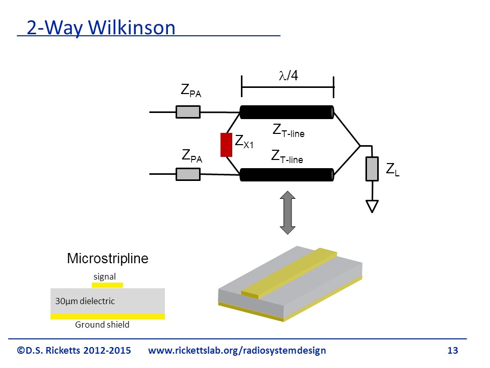
As an example, we’re going to assume that we’re using micro-strip transmission lines as shown at the bottom of the figure and that we have some source impedance. For this we use a PA, which stands for power amplifier. We want our input impedance to look exactly like our PA impedance so that our impedances match in this example. This means that we want to be equal to . Ultimately we are not only going to see how the incoming signals combine at but also how well they’re isolated from one another.
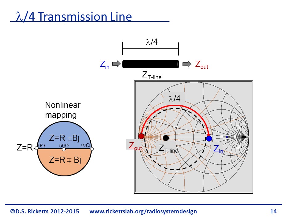
Here’s a quick reminder that a quarter wavelength transformer takes us from one side of the Smith chart to the other. Thus if we start with an output impedance as shown in red in the figure and we have a transmission line, it’s going to rotate around a quarter wavelength to the other side to the input impedance shown in blue. The black point is the geometric mean of and .
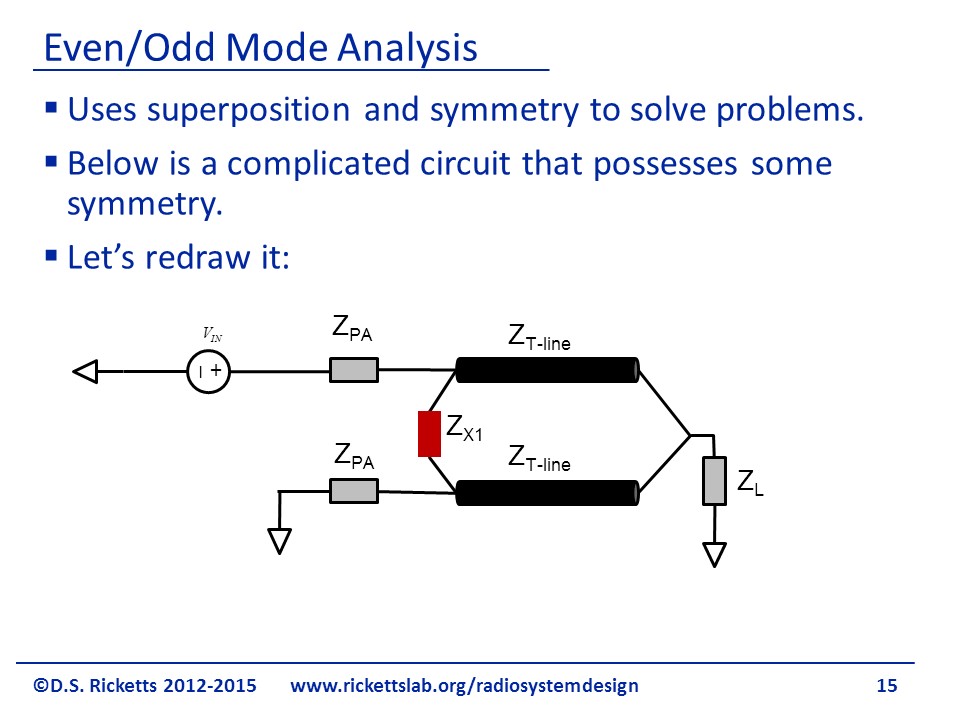
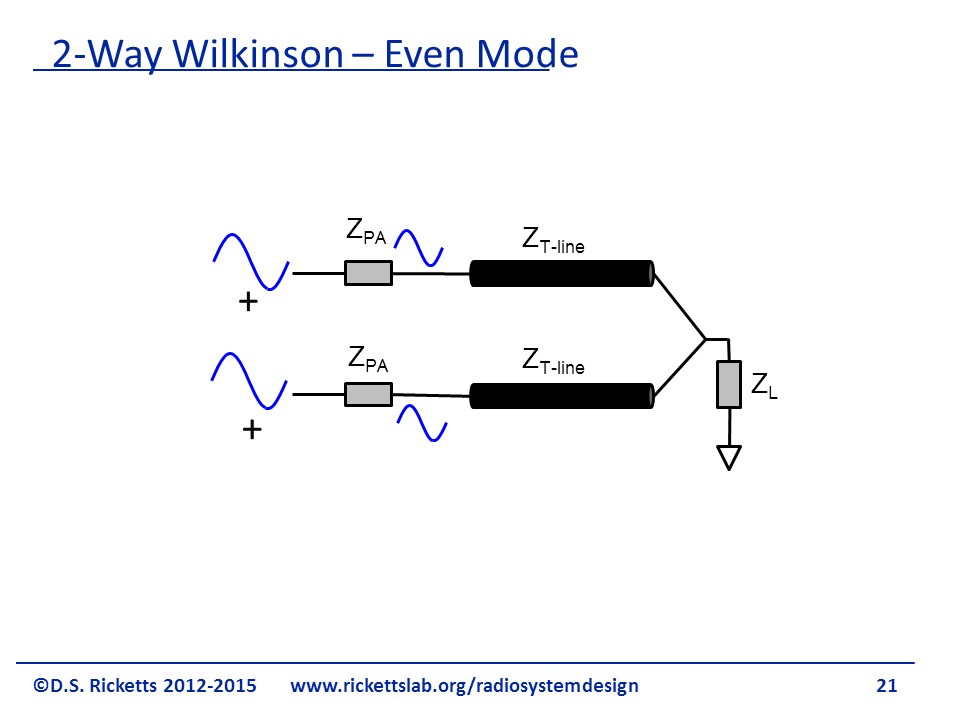
We will now discuss a concept called Even/Odd mode analysis. This technique is well-suited to solving these transmission line problems so it us used often. This method is applicable everywhere, but it’s often used in RF because it solves some difficult derivations for us. This uses superposition and symmetry to solve complex problems; the figure shows an example of a complicated circuit that possesses some symmetry. The symmetry can be seen on the right, but we want to figure out what the input impedance looks like on the left. We also want to find out what the isolation is between the two s and ideally, we would like to find the S parameters of the components on the right.
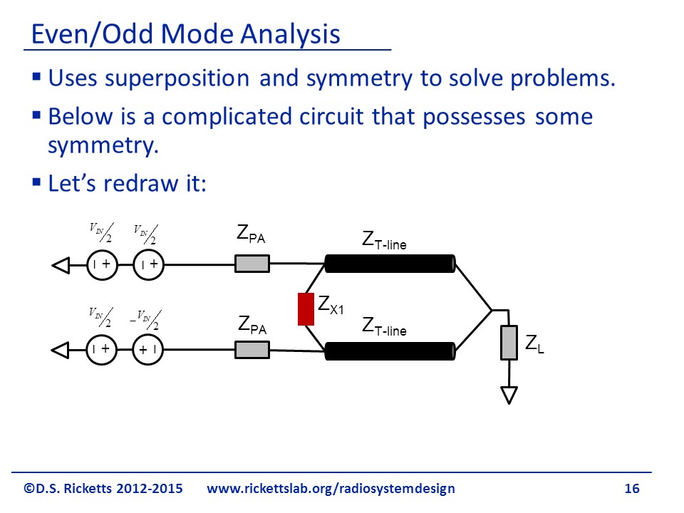
We redraw our figure as shown by splitting into two sources, and , and by splitting ground into two sources, and . Now we have two sources on each input making it a linear system, we can just look at the superposition of the effective of each set of sources.
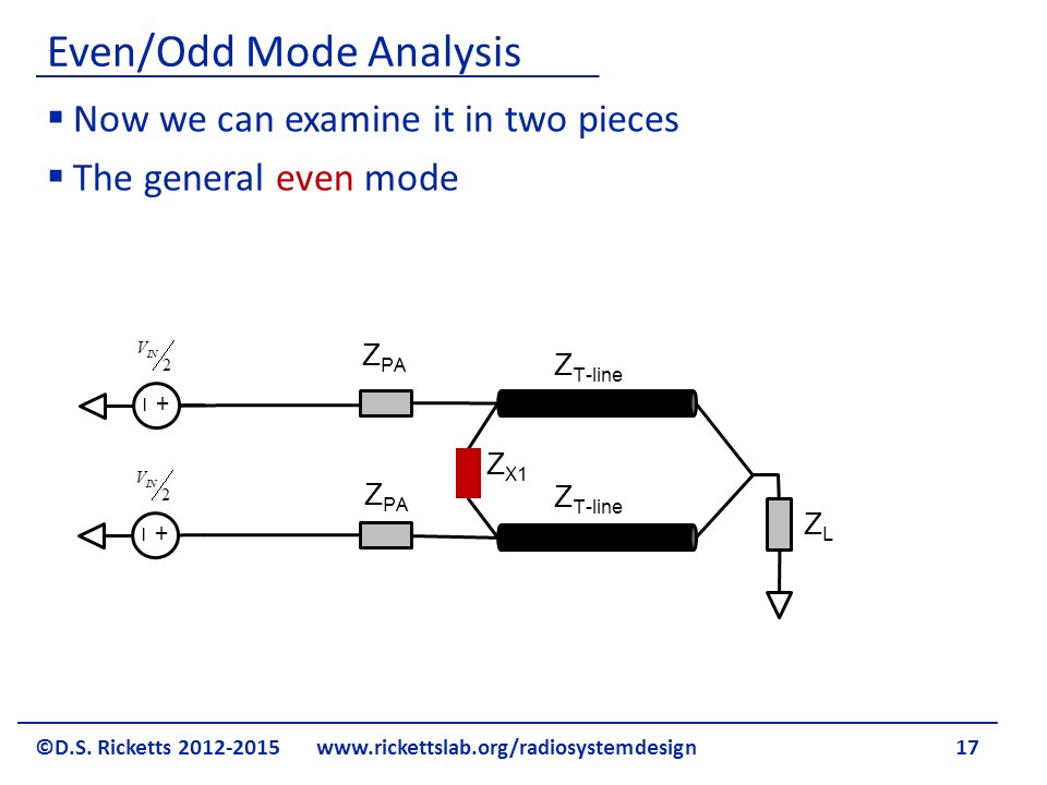
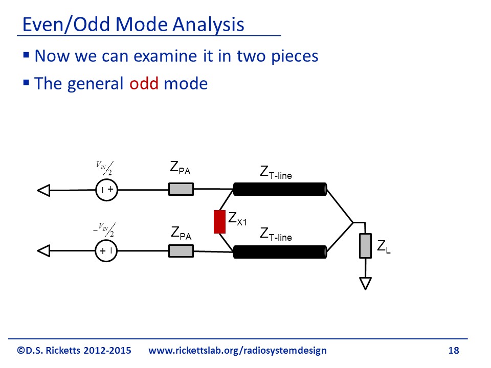
Let’s take a look at what is called the general even mode, where we’ve selected the in-phase components to see how they look. We can also look at the out-of-phase or odd mode by looking at the out of phase components of the incoming voltages.
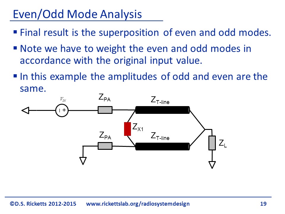
The final result is going to be a superposition of even and odd nodes, Note that when we want to solve the actual problem, we will actually have to figure out how many even and odd components our input signal has, but in our analysis to come, we’re just going to find out the general solution so that we can find the S parameters of the two port network. In this specific example, the amplitudes of even and odd components are the same because we just sum the ones at the bottom to be a ground and the ones at the top to be .

In the figure we have two in phase signals at the inputs; it’s obvious that no current is going to flow through the red resistor and so we can just remove it.
The result looks like two parallel lines with exactly the same input signals as shown.
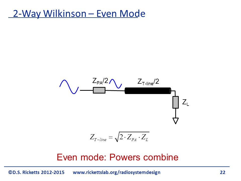
Thus, we can take the two lines and model them simply as a transmission line with half the characteristic impedance. We can find the relationship between and and the transmission line characteristic impedance we need to match to as shown by the equation at the bottom of the figure. In even mode two input signals simply combine, so this is a great power combiner.
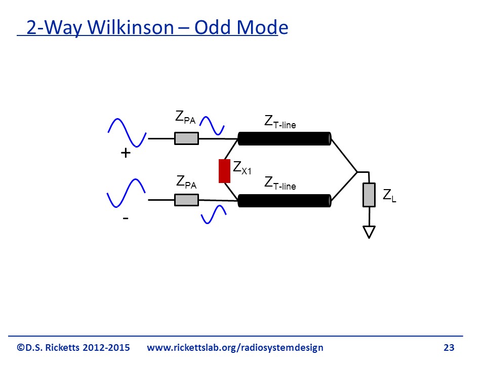
We will now examine the odd mode. As the incoming signals are out-of-phase, there is a certain symmetry right down the center. We can assume a virtual ground in the middle of the resistor and at the end as shown in the figure.
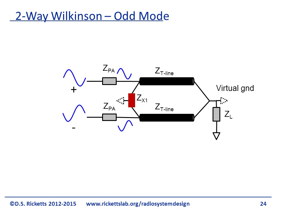
This new configuration allows us to split the original diagram into two separate circuits as shown in the figure. We can see why even-odd mode analysis is useful because when circuits have symmetry, we can find virtual grounds or virtual opens and separate them out. Note at the bottom right side of the figure that if we have a short at one end of a quarter wave-length transmission line then the other end is going to be an open.
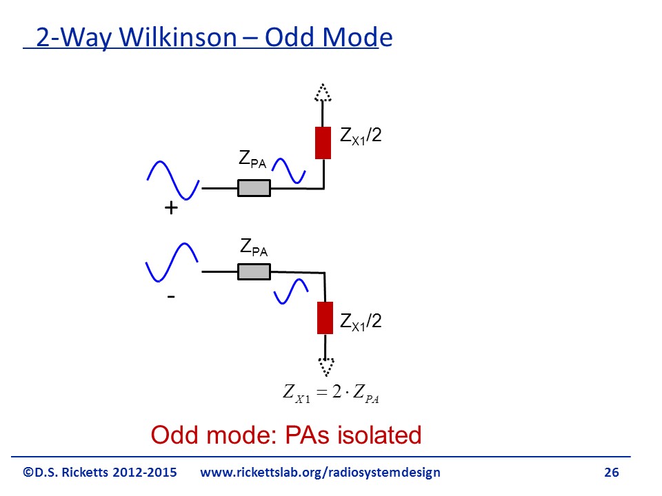
The schematic reduces even further to what is shown in the figure; so for the odd mode, we want to set equal to so that the input and the output are impedance- matched at the odd modes also t he two inputs are completely isolated from one another. To summarize, the odd mode showed us how to pick the resistor value that results in this isolation and the even mode showed us how to design a transmission line so we get the ideal and combine the powers.
Our final solution here is to put a resistor, called a balance resistor, in parallel to the split transmission line as shown in the figure on the right. This was the resistor shown in red in the previous figures.
The S-matrix of the Wilkinson is:
The first thing we notice is that , , and are all 0.
That means that the device is perfectly impedance matched. We can also see is that we have an even split between ports 1 and 2 and between ports 1 and 3. The S parameters tell us voltage and as power is proportional to , so that square root of two will turn into 1/2 and we’ll have our power divided. This can be achieved by injecting the same signal which leaks from port 2 to port 3.