
Branchline Coupler
Branchline Coupler
The Branchline coupler is a signal divider that can separate an incoming signal into two equal power, but 90 degree phase shifted signals. It consists of 4 ports: Input (P1), Ouput 1 (P2) and Ouput 2 (P3). The fourth port (P4) is terminated at 50 ohms for the signal splitter and is isolated from the input.
The branchline coupler is used to generate quadrature signals for our QAM radio.
The final PCB from the kit is 2 in x 2in, your branchline must fit on this size PCB!
Design and Simulation
In this part of the workshop you will design a 0.95GHz 3dB Branchline coupler circuit. The branchline coupler has the following parameters:
Zh: Characteristic impedance of the horizontal t-lines
Zv: Characteristic impedance of the vertical t-lines
EL: electrical length of transmission line
Z: impedance of the 4 ports
F0: operating frequency
Ideal Transmission Line Implementation
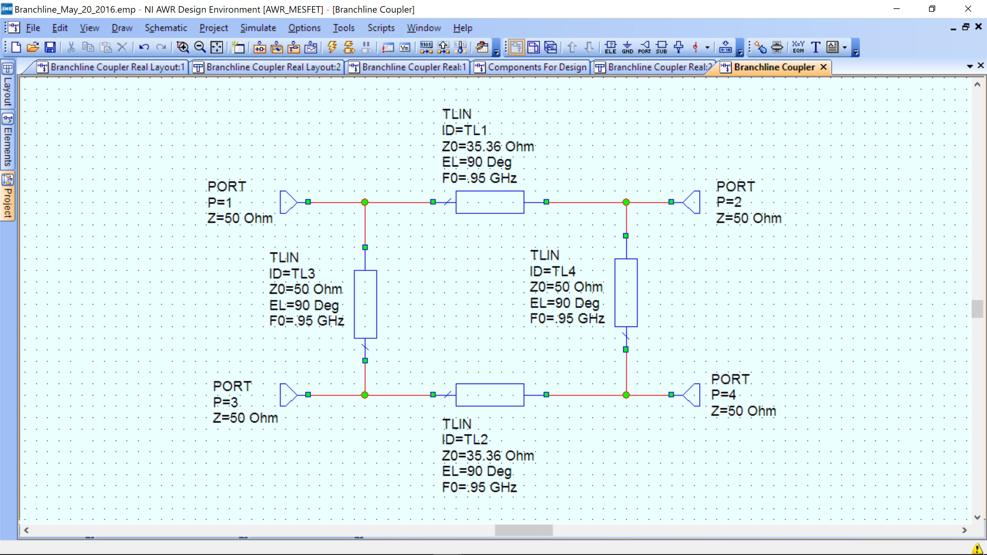
Create a new schematic design and call it “BranchLine ideal”. Add four TLIN elements and four ports and connect them as shown below. TLIN is an ideal transmission line specified by electrical length and impedance – it does not have a physical representation. Set Zh=35.36Ohm , Zv=50Ohm, EL=90deg, Z=50Ohm, F0=0.95GHz.
Components can be added as follows:
- PORT and GND can be added directly from the tool bar at the top of the software (labeled “PORT” and “GND”)
- All other elements can be added by Ctrl+L then type the name of the element, e.g. RES or CAP, and you will find it in the list that appears.
- Special components: MVIA1P (special via to ground) must be copied from the Design for Components Schematic in the template provided.
Setup the simulation by going to Options->Project Options->Frequencies and setting the range from 0 to 4 GHz in 0.01Ghz steps. Hit Apply and make sure replace is selected.
Add a Rectangular graph, Project->Add Graph. Then Right-Mouse Click->Add Measurement.
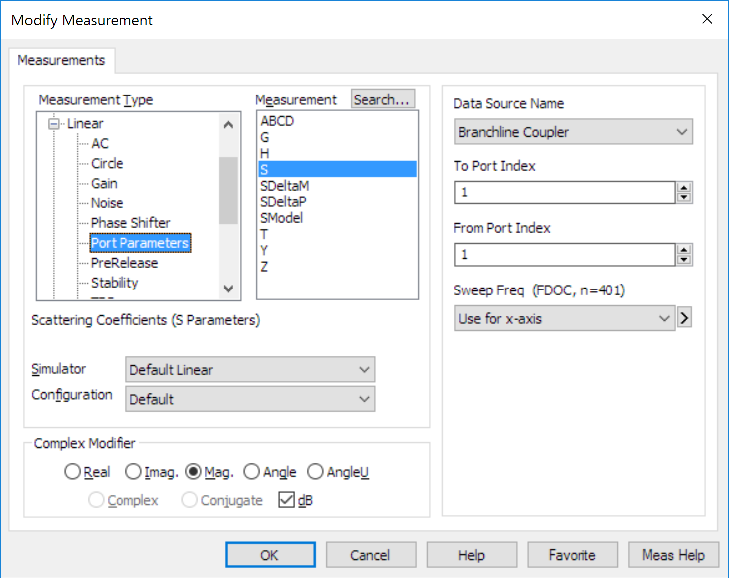
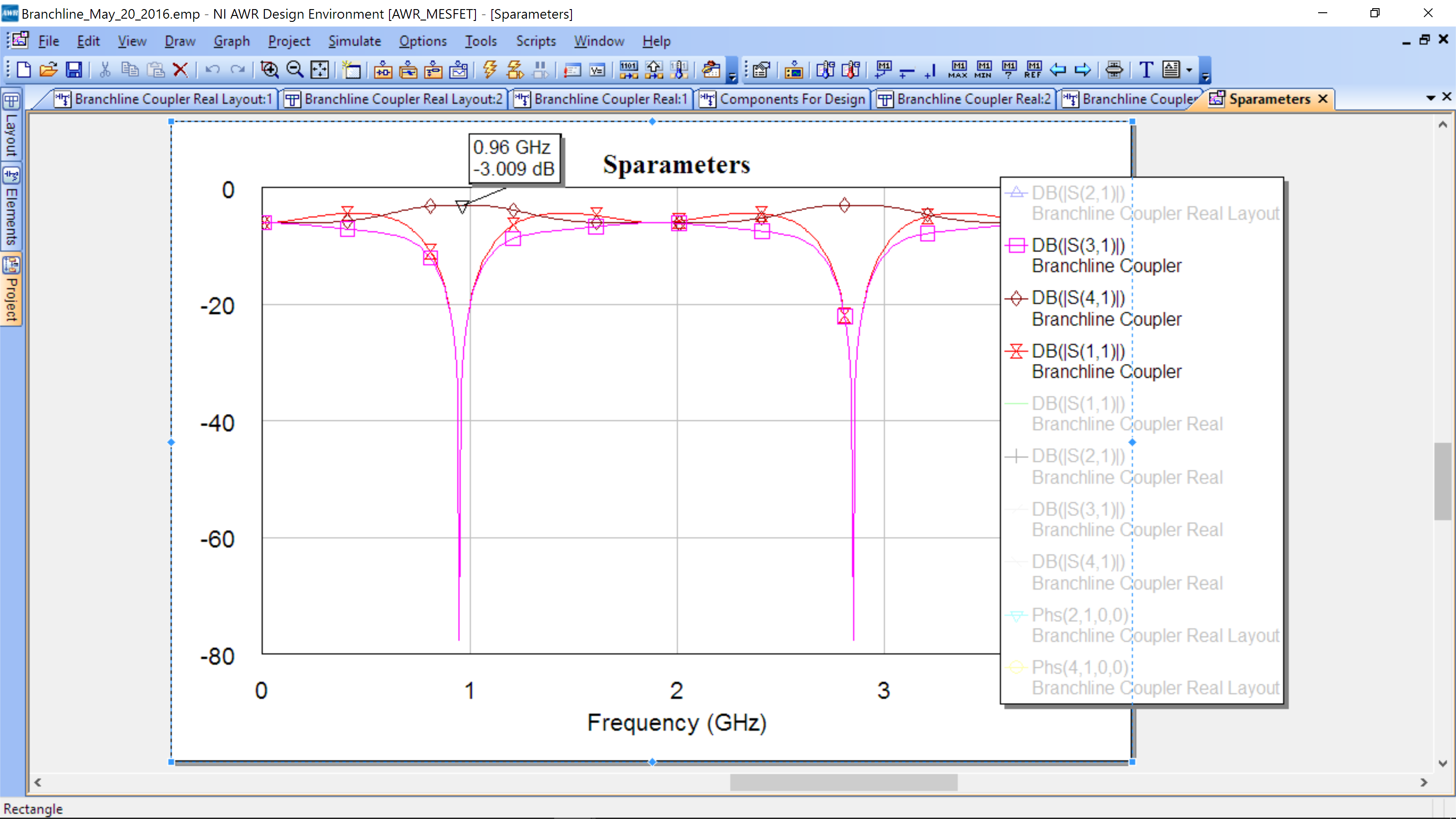
Add a measurement of magnitude of S11 (port 1 to port 1), S21 (port 1 to port 2), S31 (port 1 to port 3), and S41 (port 1 to port 4) in dB scale. Add marker on S11 and S31 curves at 0.95GHz. You should see the image below with similar magnitude values.
Real Transmission Line Implementation
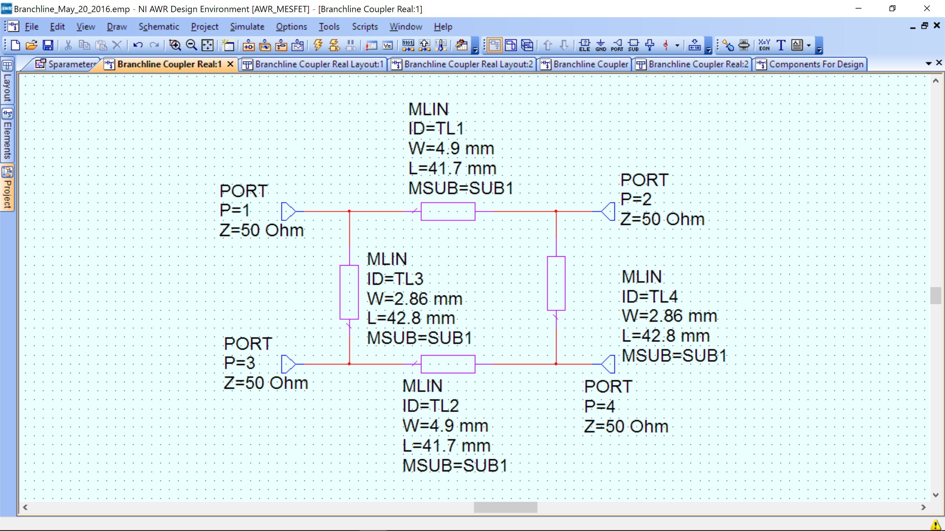
Create a new schematic and call it “BranchLine real”. Add four MLIN elements, four ports. MLIN are transmission lines with a microstrip transmission line realization – this model incorporates the non-idealities of a microstrip transmission line and depends on the specific stackup of your substrate. The MSUB from the Global Definitions has the correct information for our workshop. Do not add an MSUB block!
Determine the Width and Length of the transmission lines using TXLINE and bulid the real Brachline coupler schematic. TXLINE can be found under Tools-TXLINE. It is a calculator to help you convert electrical parameters such as electrical length and impedance to a physical implementation. The following screen shot show the calculator interface.
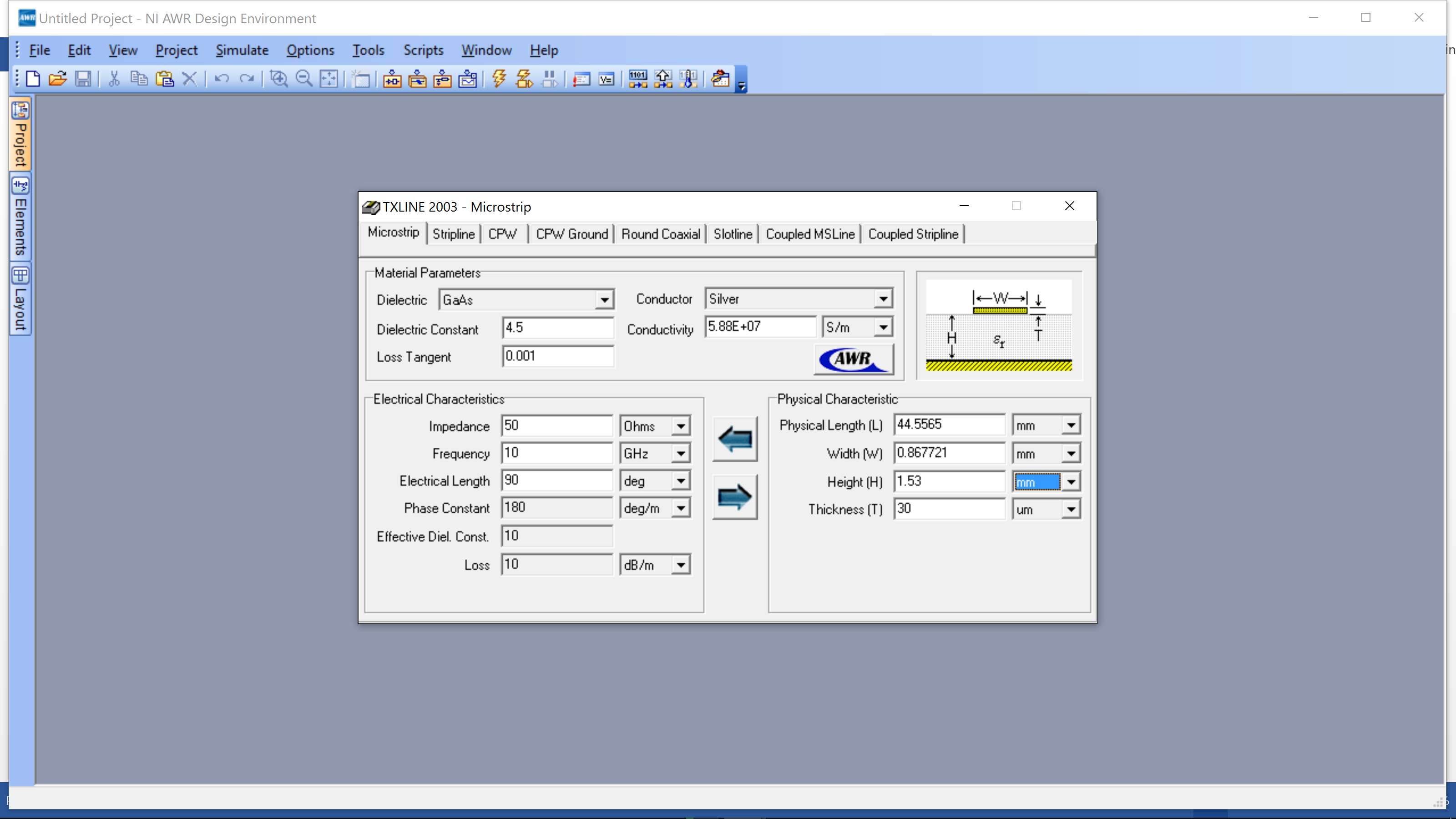
The picture shows a transmission line with a 50 Ohm impedance and an electrical length of 90 degrees at 950 MHz. The calculator works bidirectional. To find a transmission line from electrical length, insert all of the the parameters on the left. Also set Dielectric Constant=4.5, Conductor=Copper, Height=1.53 mm, Thickness=18um. These are obtained from the PCB stackup we are using in the workshop. Note that the Height and Thickness are set on the right side, even though we are calculating from left to right in this example. Click the right arrow – it will calculate the width and length to the line. Likewise, if you change the Length or Width on the right side and click the left arrow, it will calculate the new Electrical Length and Impedance.
Note: length and width should only have two significant digits, i.e. 2.35 not 2.357.
Your schematic should look similar to the one below.
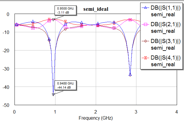
Set simulation frequency range from 0 to 4GHz with steps of 0.01GHz. Plot the magnitude of S11 (port 1 to port 1), S21 (port 1 to port 2), S31 (port 1 to port 3), and S41 (port 1 to port 4) in dB of the real Btanchline coupler model in Rectangular graph. Add marker on S11 and S31 curves at 0.95GHz. (1 pts). The result should look like the figure below.
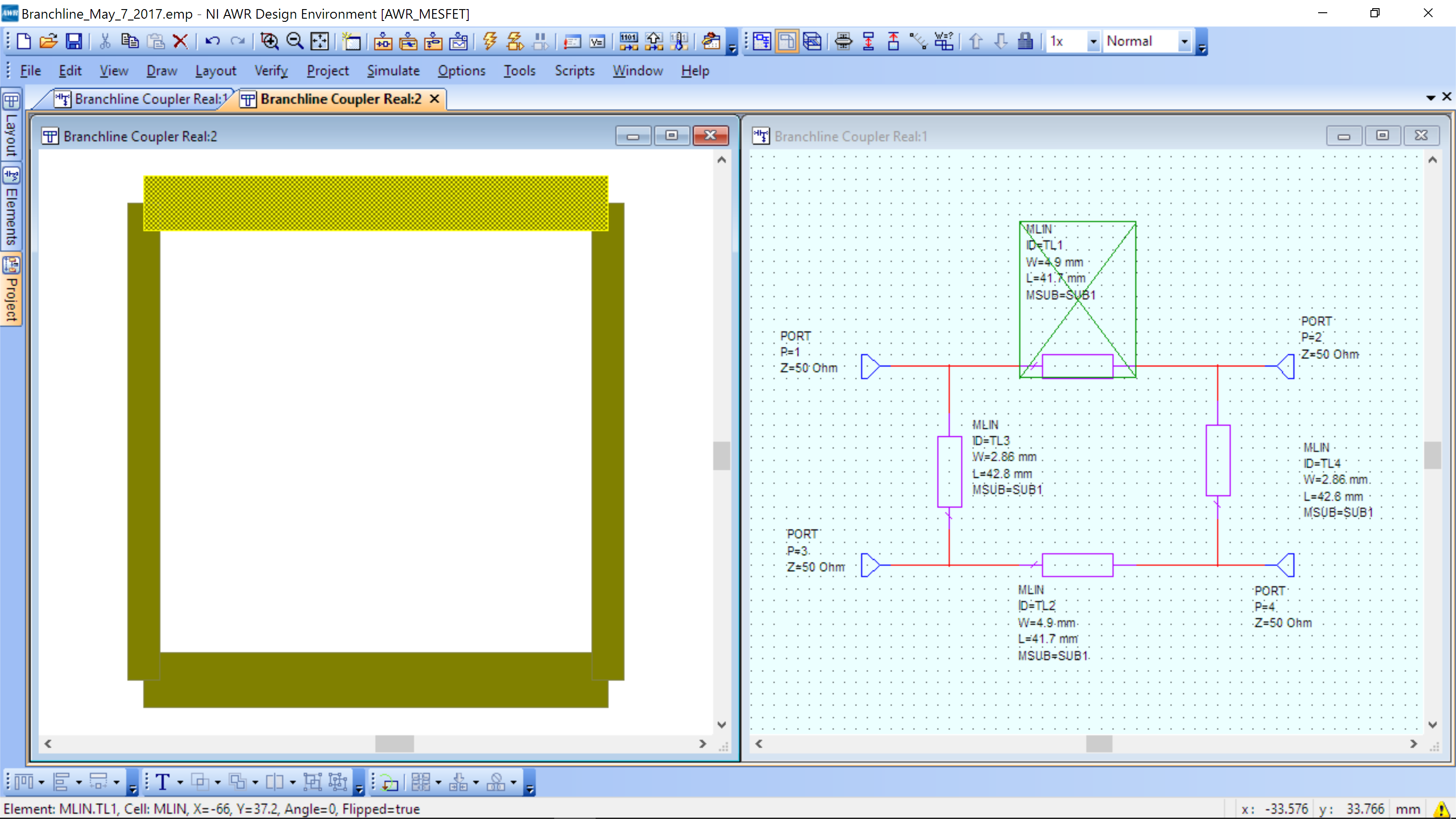
Right click on the “BranchLine real” under the Circuit Schemtics in project browser and select View Layout. The layout window will open and below is an example of how it may look like.
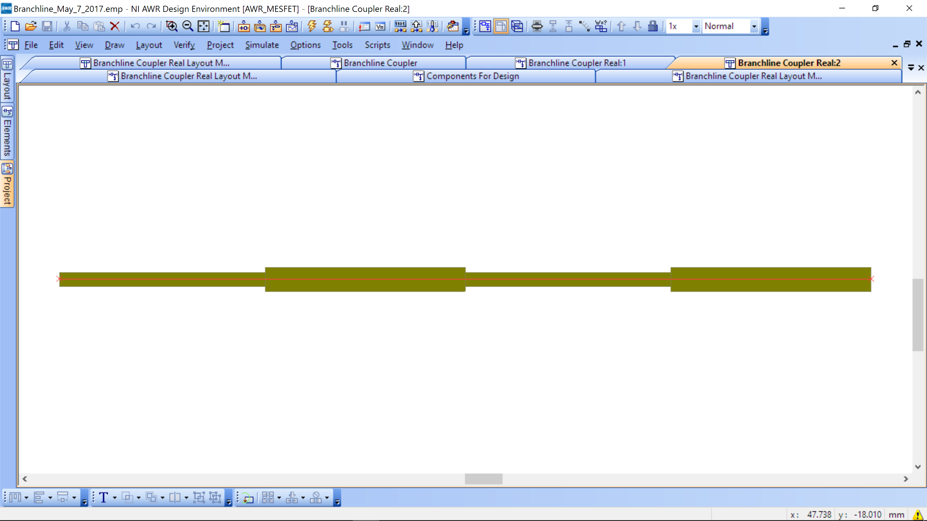
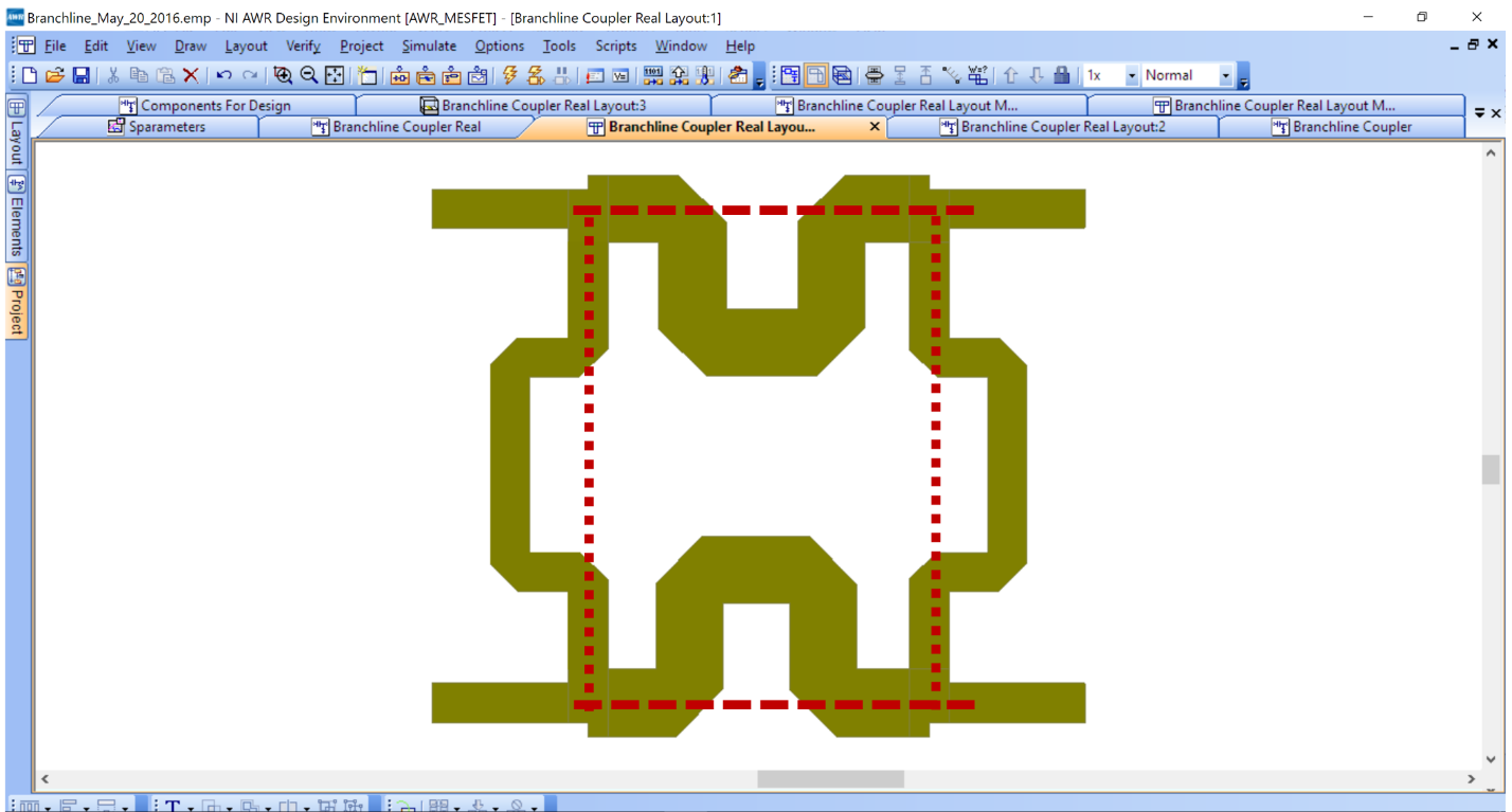
This means orientation of the 4 transmission lines with respect to each other is not known even though you placed them perpendicular in the schematic. The red dashed lines indicate where an electrical connection is made. You can select one of the lines and move it around with your mouse and you will see that the red lines still show the correct electrical connection.
Try to re-arrange the lines, and rotate them to the correct orientation until all the red lines disappear. You can rotate elements by Ctrl-R (or access through th Edit menu). If you are confused which component in the layout correspond to which transmission line in the schematic, you can have both schematic and layout views side by side, and see that every time you select an element in one view, its corresponding element in the other view is highlighted. If you placed everything correctly your final layout should look like this.
As you see lines overlapp which each other in the corners resulting in the effective length of lines to be shorter than what you specified. Also there are discountinuities where lines meet, and there is no clear point where input and output connectors (represeted by ports in the schemtaic) should be attached on the PCB.
In order to fix these problems we will add a few new components to the schematic.
MTEE$ – A T-junction with three edges widths W1, W2, and W3. The width of W1, W2, and W3 is set automatically to the same width of tline which T-junction is connected to.
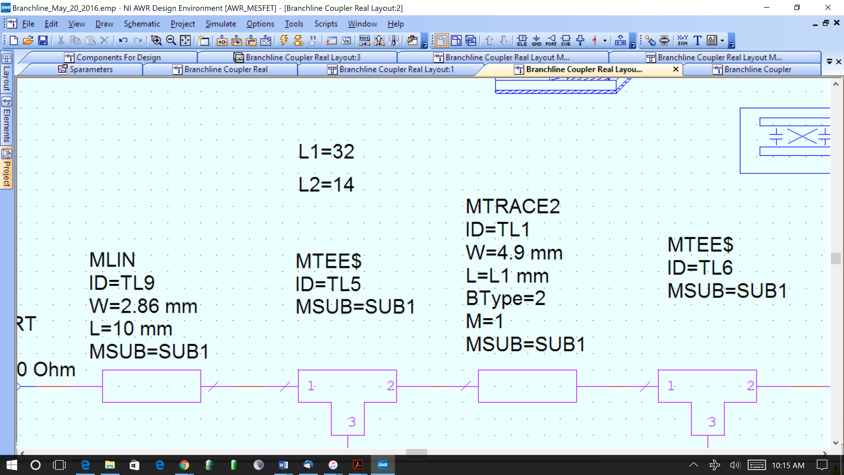
Also lets add short pieces of additional microstrip line MLIN between each port and T-junction. Ue TXLine to find a 50 Ohm width. If you keep characteristic impedacne of these transmission lines to 50Ohm, they will just act as extention to the 50ohm ports and will not affect performance of the coupler. Schematic of the modified real Branchline coupler is shown below.
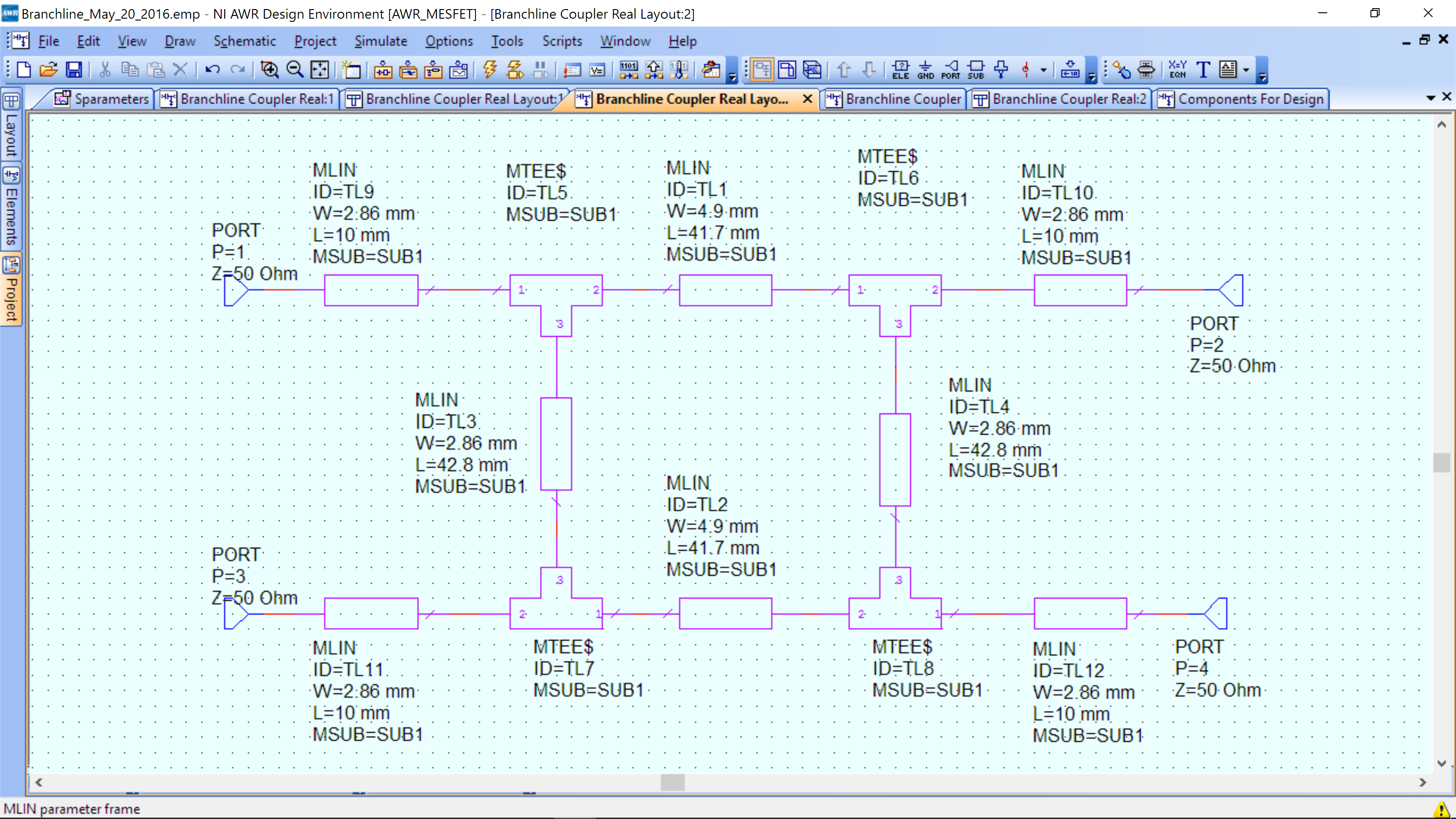
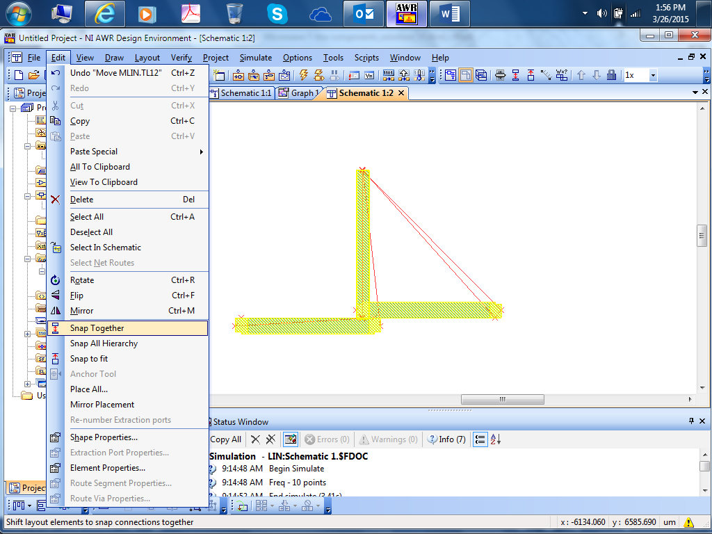
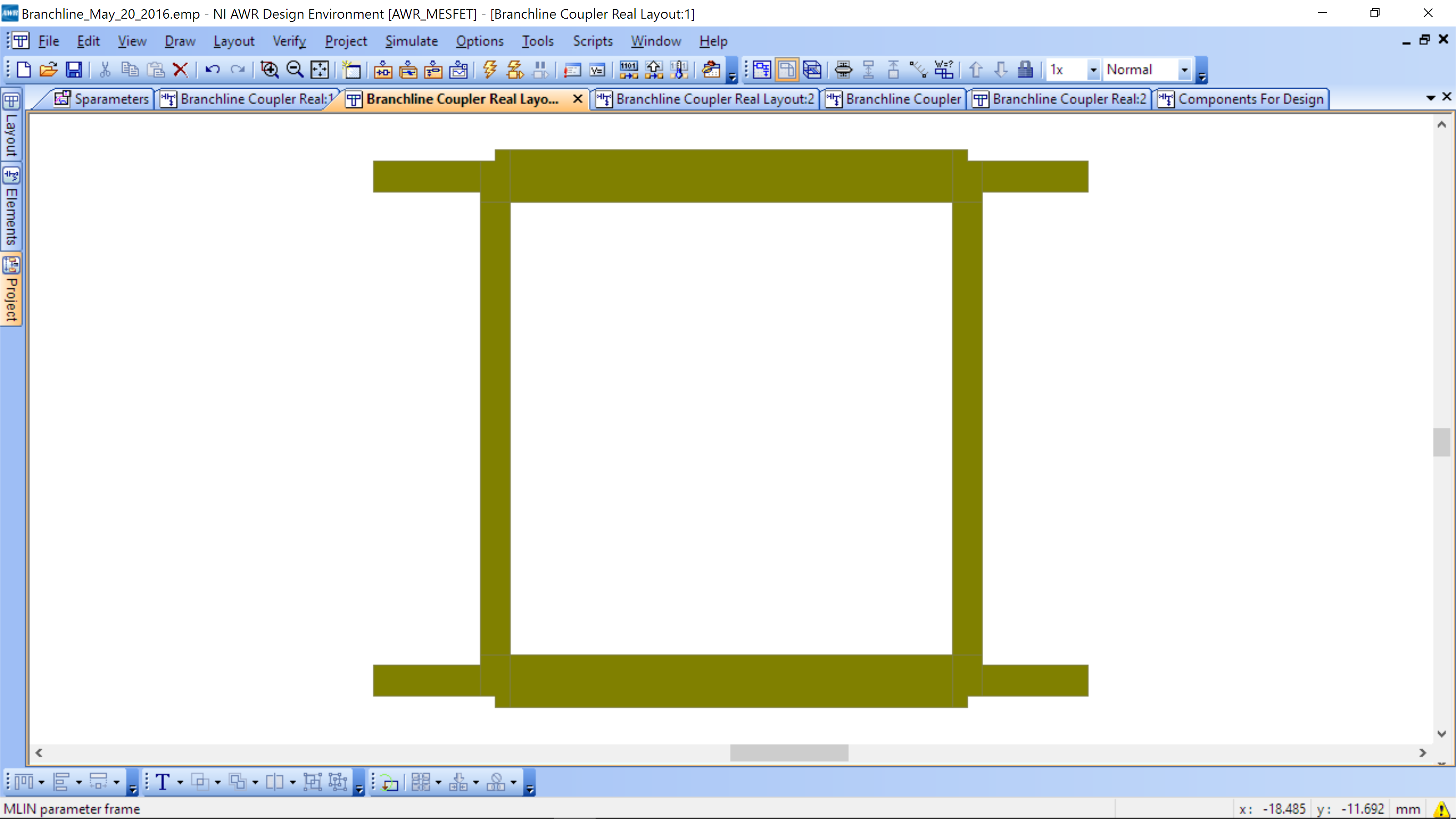
Try to view the layout of the Branchline coupler now. As shown in the figure below, lines are at correct orientations but still not properly arranged. Select all the components (Ctrl+A) and under edit menu select Snap Together. This will re-arrange the lines to form the final layout of your coupler.
You can also see the 3D view of the layout by clicking the following icon (seen when the layout window is active)
 .
.
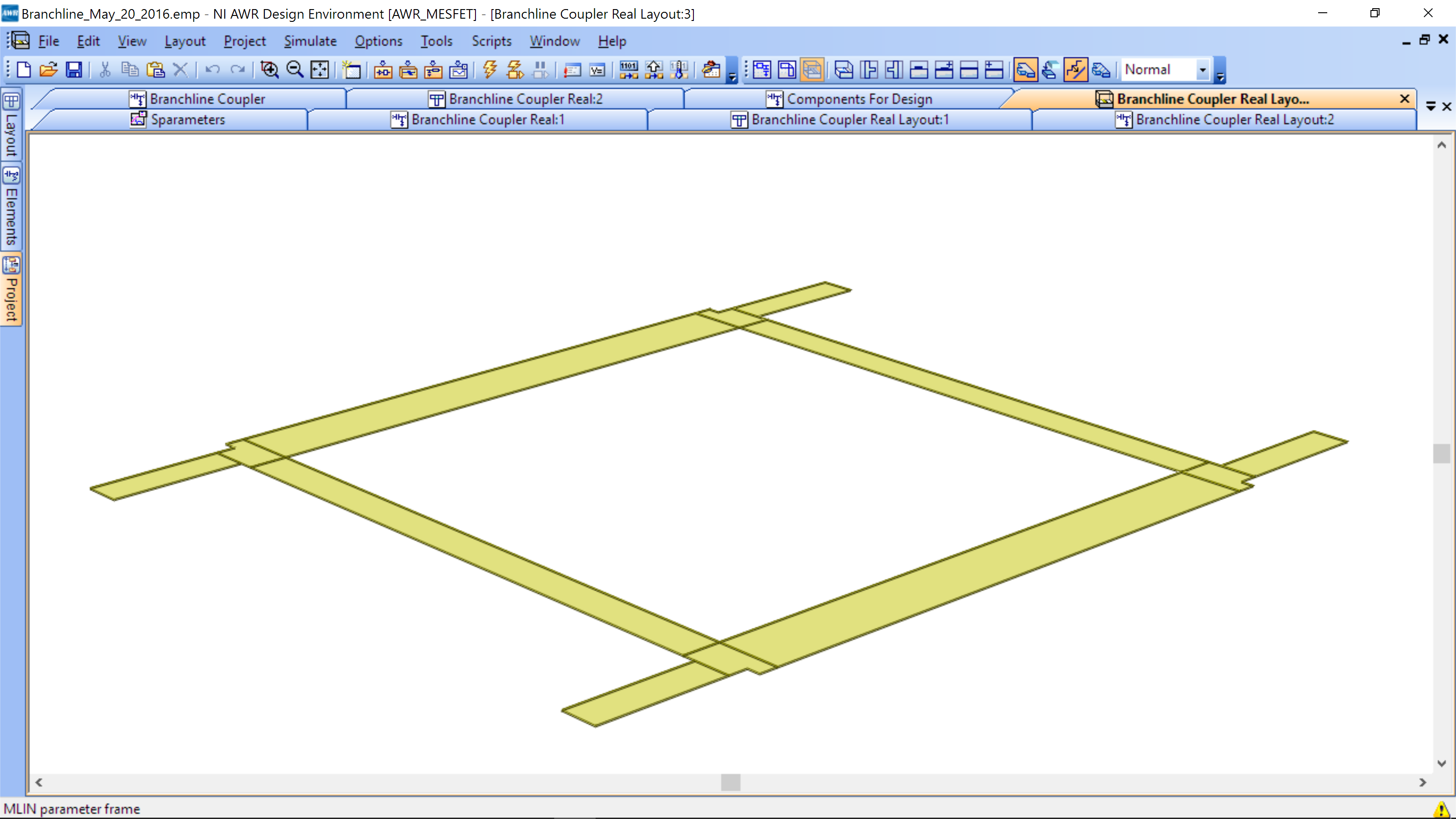
The 3D layout is below.
EM Transmission Line Implementation
Note that generating and correcting the layout does not affect the simulation results of the coupler, since AWR uses the symbols in the schematic view and the layout view. It is however important to have the correct layout of the coupler for EM simulations.
For those who have used AWR before, the substrate definition is hidden in the Projects->Global Definitions and is called SUB1. You should not add any additional substrate symbols to the schematic.
To perform an Electromagnetic simulation of the coupler, go to Scripts->EM->Create Stackup this will setup the schematic for EM simulation. Your schematic should have the Stackup and Extract components in it:
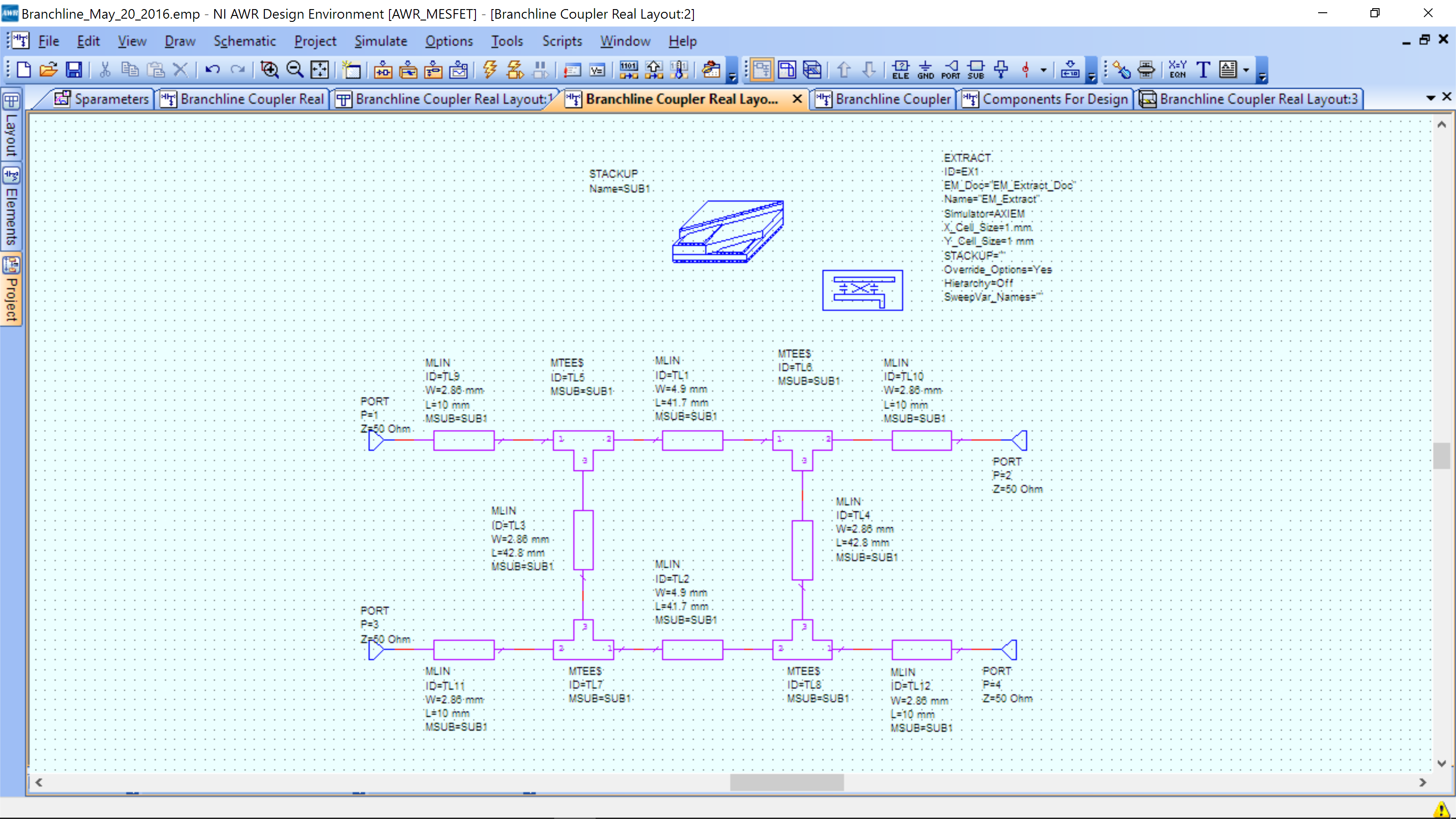
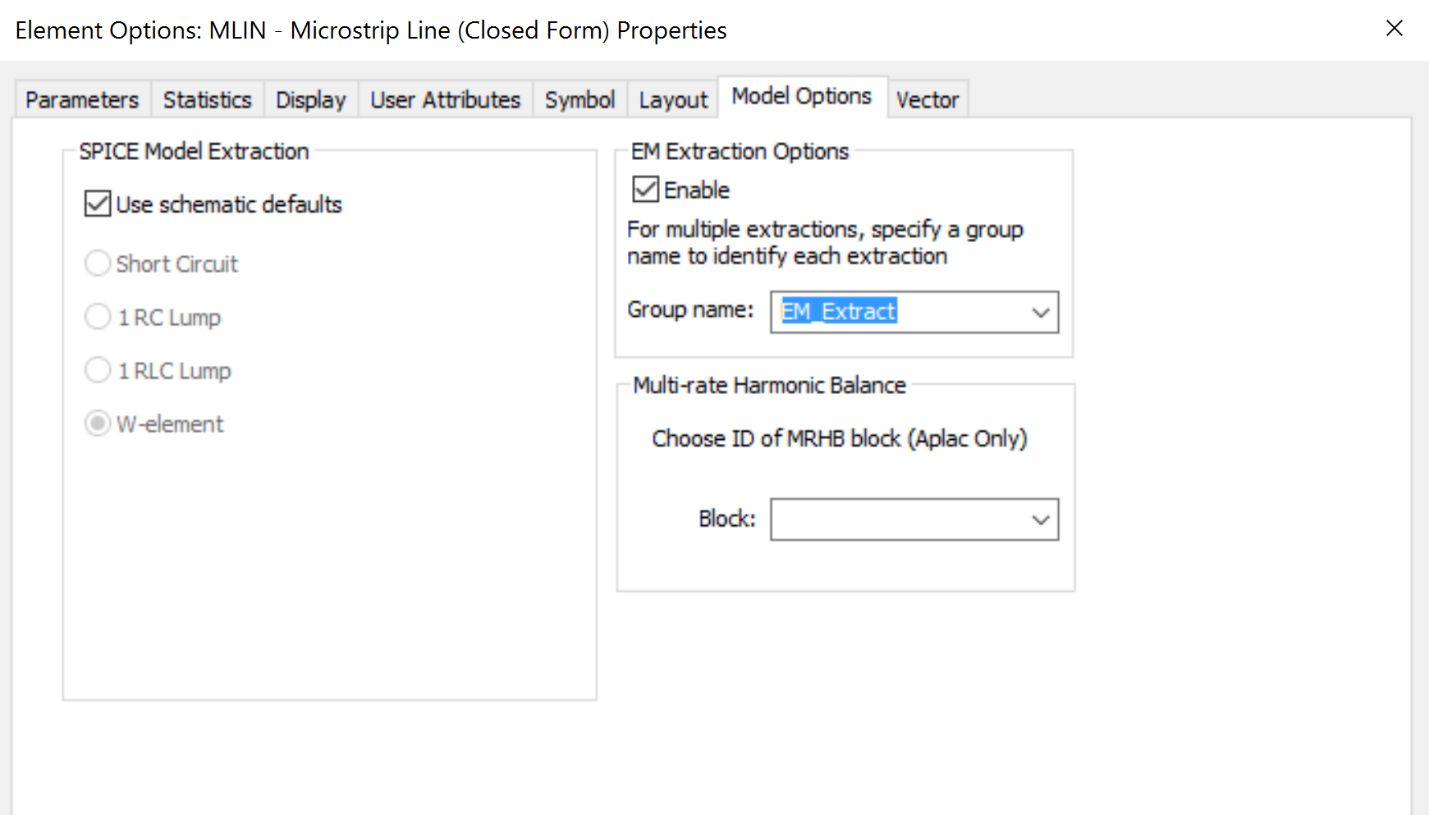
Now select all of the tline components (use Shift and mouse button to select several at one time). Then Right-mouse Click->Model Opetions and enable EM Extract.
When you click on the Extract element, everything that is being extracted should turn red. Your circuit should look like the one below. This figure has used Window->Tile to show both the layout and schematic. The schematic and layout are linked, so both turn red.
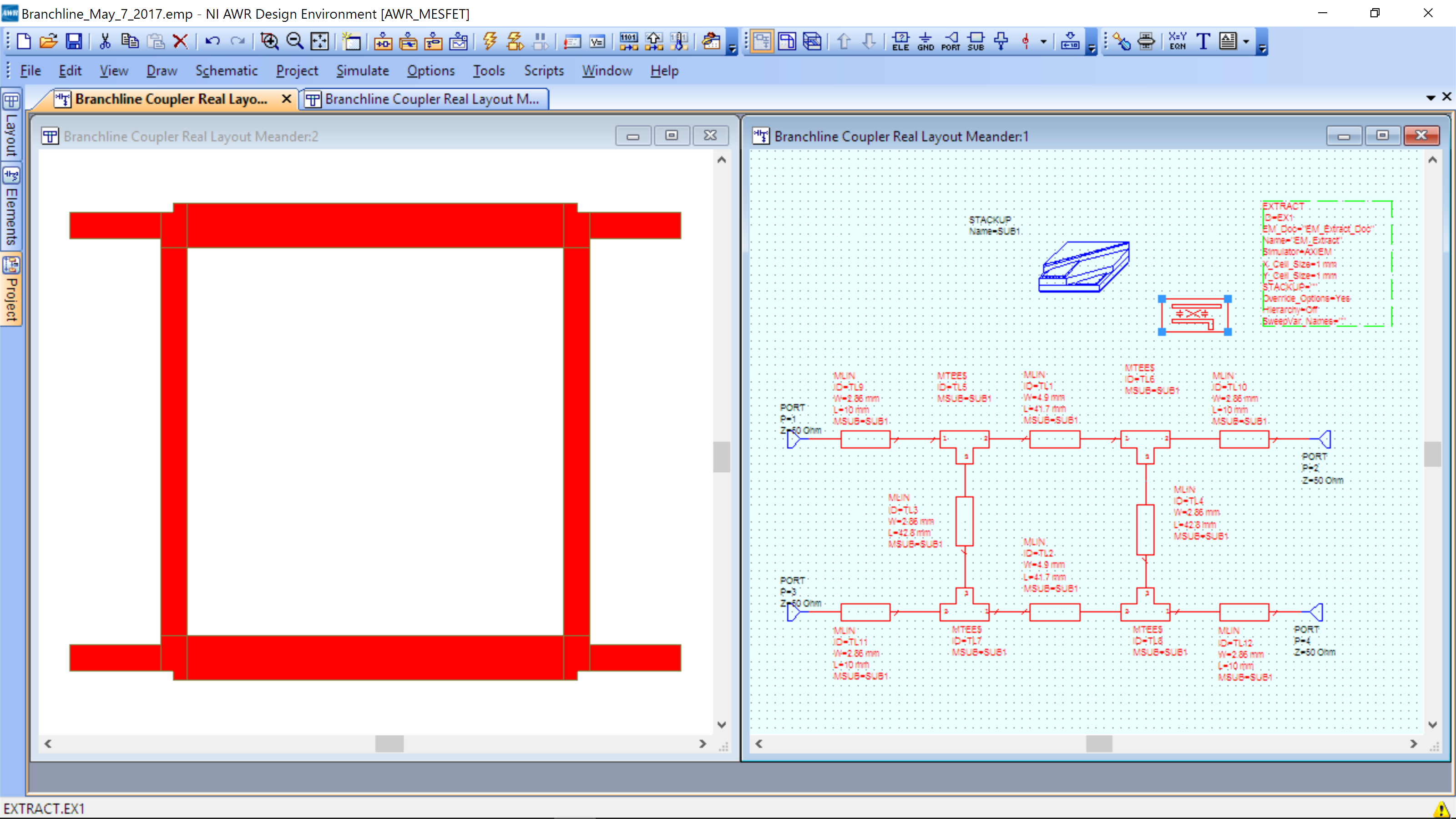
NOTE: The ports are blue and are not extracted (there is not an EM model for them).
You can now rerun the simulation and an EM extraction of the exact layout will be done and the simultion results updated with the new results.
IMPORTANT: Your simulation will take a very long time if you do not perform the following:
In the Extract component text (just double click directly on schematic), set the X_cell_size=0.3mm and the Y_cell_size=.3mm. Then right mouse click on the Extract block, and go the the frequencies tab, set the EM simulated frequencies to .55 to 1.55 by .1 GHz steps. Make sure the Use Project Defaults is unchecked. This allows you to run your EM simulation on fewer points for faster simulation.
You can now re-run the simulation and an EM extraction of the exact layout will be done and the simulation results updated with the new results. When using MLIN and straight layouts, very little difference will be seen. This means the MLIN component is already modeling the EM effects accurately. The difference will be more significant when using meandered transmission lines, lines that are close to other structures and non-transmission line conductors, eg. Ground plane.
The extract simulation results should looks similar to those below.
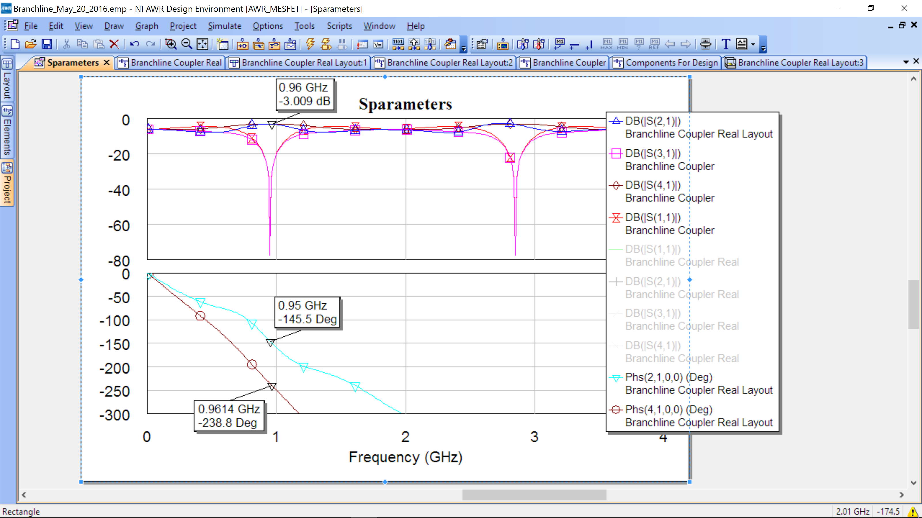
Note that we have added the phase out of each port. They should be 90 degrees apart.
The final PCB from the kit is 2 in x 2in, your branchline must fit on this size PCB!
Next we will replace the MLIN model by MTRACE2. You can do this by just changing the name of the component in Schematic view. You will notice that the layout view is not changed! There is a difference however. Hover you mouse over one of the lines in the Layout view, you will see an arrow on one end (see figure (a) below).
Return to the schematic and tybe Ctrl+E (equation) which will bring up a text like cursor. Place it somewhere on the schematic and type in L1=XX, where XX is the length of one of your MTRACE2 lines per your design above. Then double clicke on L on the top MTRACE2 text and change the numerical length to “L1”. This doesn’t change anything in the simulation, but does in how the layout handles the length of MTRACE2. Do the same for an “L2” for the right/left lines.Here is an example (L1 is for top/bottom and L2 is for left/right transmission lines.) The lengths are arbitrary in the picture (not the correct design lengths).
Go to the layout. Now double click on the line, three handles appear at the beginning, middle and end of the line. Double click again on the handle which is at the end where the arrow/triangle is and you will notice that your cursor changes to a drawing path (see figure (b) below). You can now draw a path, for example to meander the line (see figure (c) below). Once you are happy with the shape you want the line to look like double click and the line will be re-drawn according to your path. (see figure (d) below)
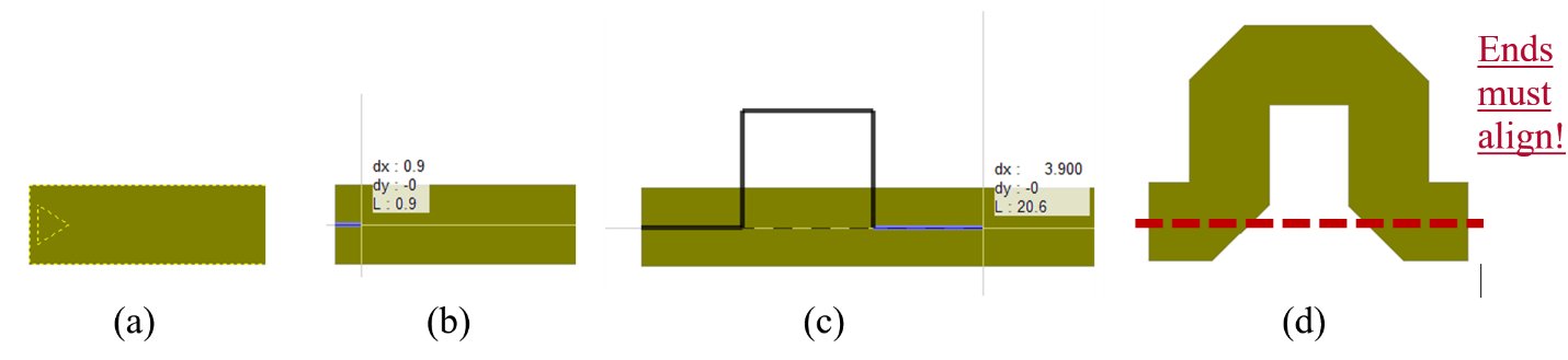
Notice that by doing this meandering the length of the line has not changed! This means the software will adjust the drawing in X and Y direction so that the total length remains constant – this is because of our use of the equation for “L1” and not the number in the L parameter of MTRACE2. This also means if the path you draw is longer than L1 of the MTRACE2 you specify in Schematic, the meandering shortens the line to the defined length. Also note that even though you changed the shape of the line in Layout the symbol in the Schematic is still one straight line. Once the line is meandered, you can adjust the spacing and extension by double clicking on it and moving the handles.
An example meander is shown below. Note that it is much shorter than the standard line.
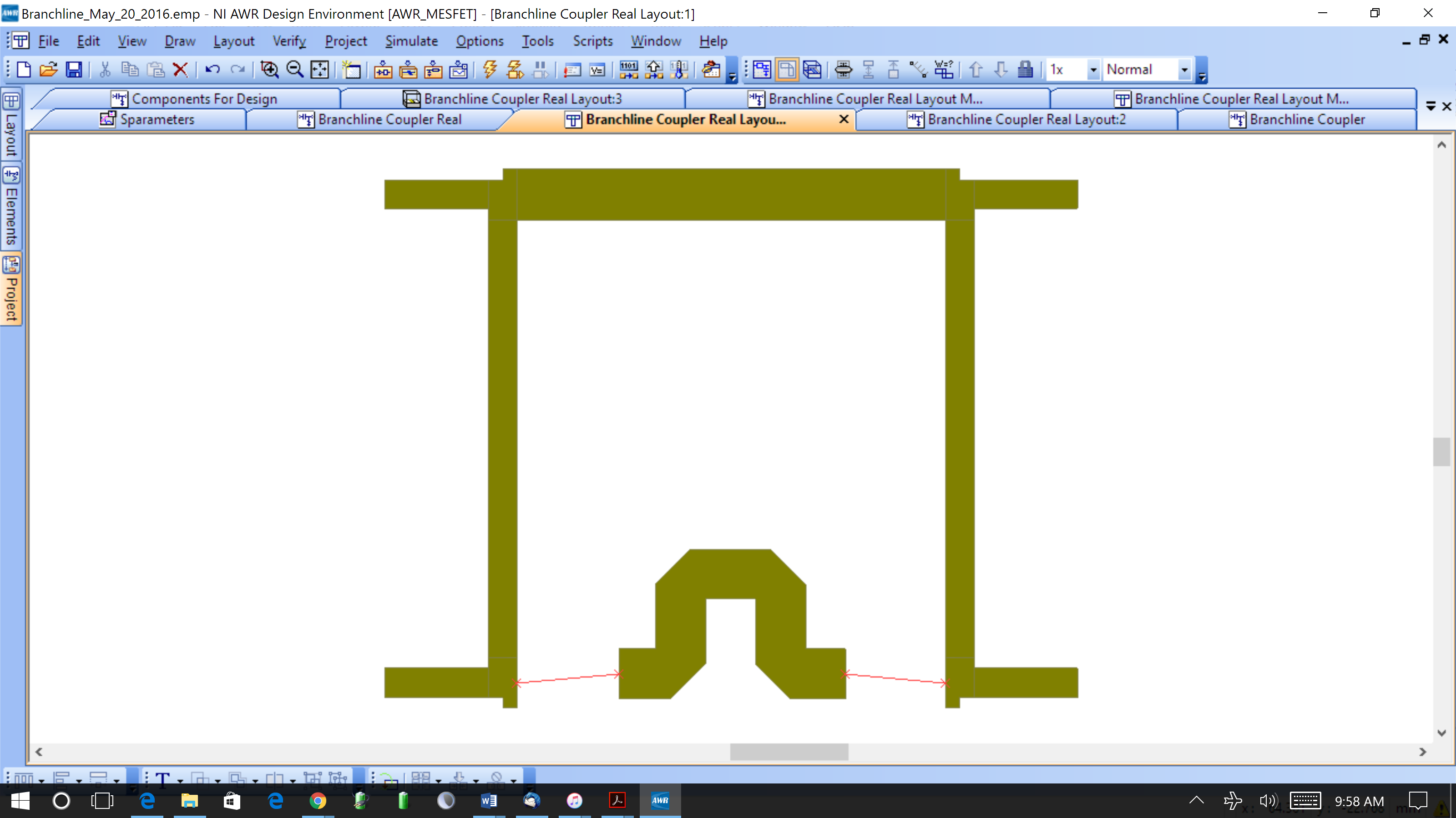
Meander all the four lines in your Branchline coupler. Note that you only have to set an L1 and L2 as two lines have the same length and you can reuse the parameter equation L1=XX. A typical suggestion is shown below. Yours may look different and that makes every design unique!
For the Branchline coupler it is critical that the ends are aligned, as shown by the red dashed line in the figure above. This is to ensure they will connect to the other 3 lines in the coupler.
Trick: Meander the top and left transmission lines. Then go to the schematic and delete the bottom and right transmission lines and copy and paste the top to the bottom and the left to the right. This way the left/right are identical layouts and so are the top/bottom. You can use “Mirror” in the layout to create mirror images and then assemble all 4 transmission lines together.
By ensuring that: 1) you have the ends aligned for each transmission line and 2) you copy and paste so left is identical to right and top is identical to bottom, your layout will be very simple.
There is no need to meander the four 50 Ohm line which were added outside of the coupler. You will solder the SMA connectors directly to those 50 Ohm line.
Select all the components in the Schematic view, right click and in Properties>Model Options make sure they are added to the Extract group. Run the simulation. A new EM simulation will be set up and run. Compare your results to the previous simulations.
Note: If your simulation does not run, your layout may not have all the edges touching. Check for any red “x”. You can also use the Snap Together to try to make sure everything is connected, however if a connection is not possible, a red “x” will appear.
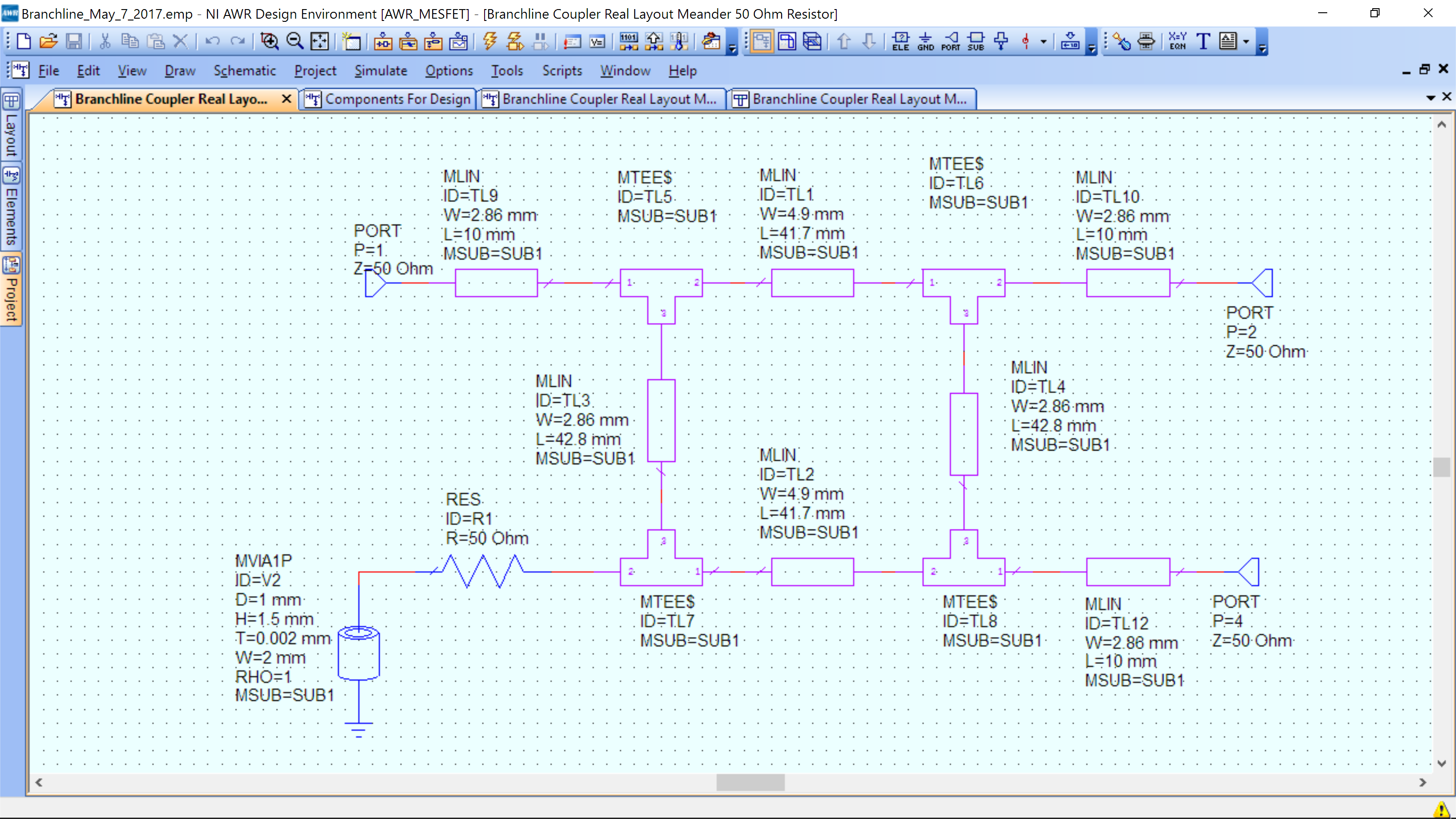
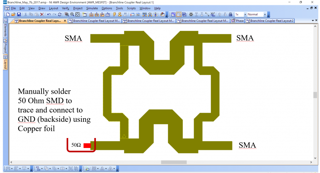
In your final circuit, PORT3 of the coupler will not be used, it will be terminated to a 50Ohm load. While this can be done with an SMA termination it is better to have a 50Ohm resistor on the board.
To do this go back to your Schematic view, remove PORT3 and add an MVIA1P from the Components for Design schematic that can be found under the project tab to the left, subsection Circuit Schematics. Copy and paste it over and enable it by Right-mouse Click-> Enable. This is the via that will allow you to connect to the ground plane on the back of your board. Then add a 50 Ohm resistor (Ctrl+L, Res) between the via and your branchline. The finished circuit is shown below.
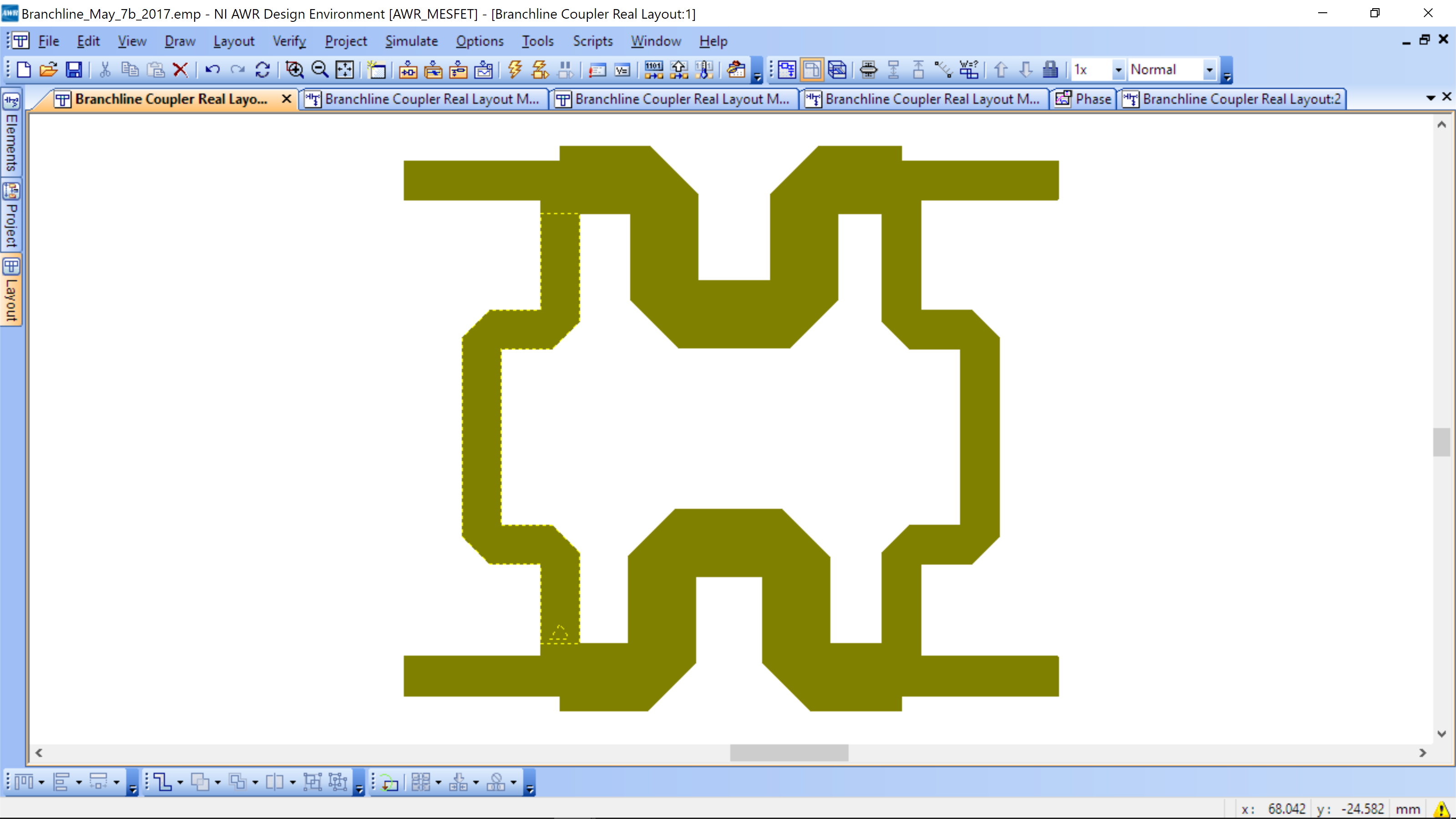
The 10mm 50 Ohm transmission line was removed, but could have been left in the design. The resistor does not yet have a layout. To add a package: Right-mouse Click->Layout->Library Name->Components. Then select 805 for the package type. The final layout looks like this:
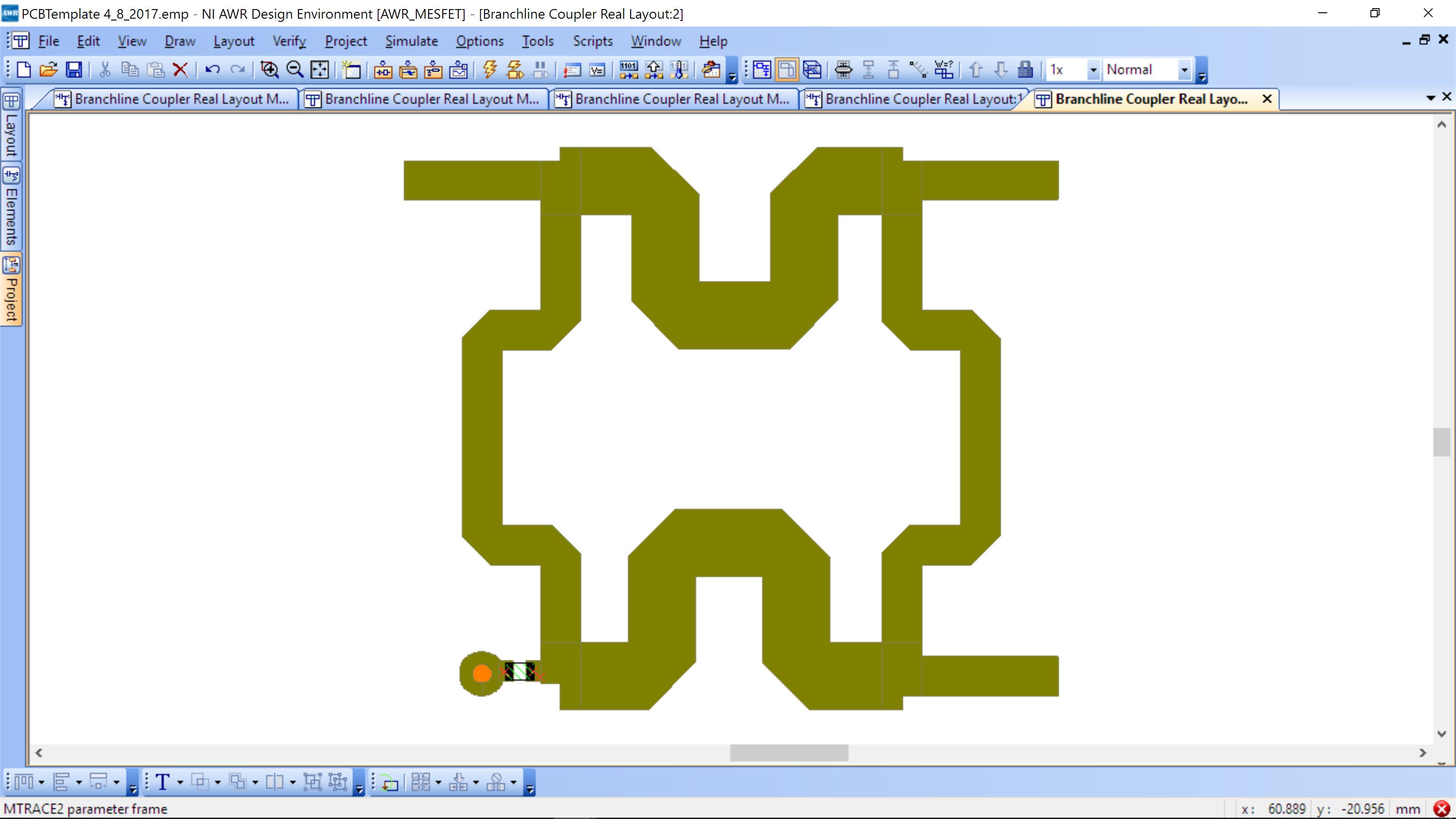
The red “x” by the via indicates that the layout does not “see” the connectivity. Make sure to zoom in and see that the resistor pads touch the coupler and the via. The red “x” will not go away, so you have to verify visually.
Fabrication – 2D Cutter
To prepare your design for fabrication using the 2D cutter, add a 50 Ohm transmission line back on port 4, where you put the 50 Ohm SMA resistor. You will solder the resistor to the transmission line and connect to the backside (gnd) with copper tape (not shown).
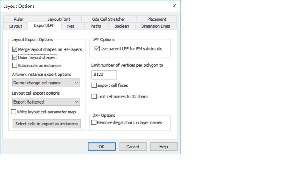
Go to the menu and select Options->Layout Options. The following window appears. Make sure to select “Union layout shapes” and deselect “Subcircuits as instances” if selected. This will merge all of the shapes upon export. This is necessary for the cutter fabrication.
Now export the file, Layout->Export-> set save as type as (DXF, Flat,*.dxf). Save your file with your name, e.g. Power Amplifier_
ricketts_V1.dxf. Take your file to the 2D cutter for cutting of the copper top layer of your board.
Note: Two files will be created, one is the name.dxf file and another is a name.dxf.txt file. Please send the .dxf file to the person working the cutter. The .txt file is not used.
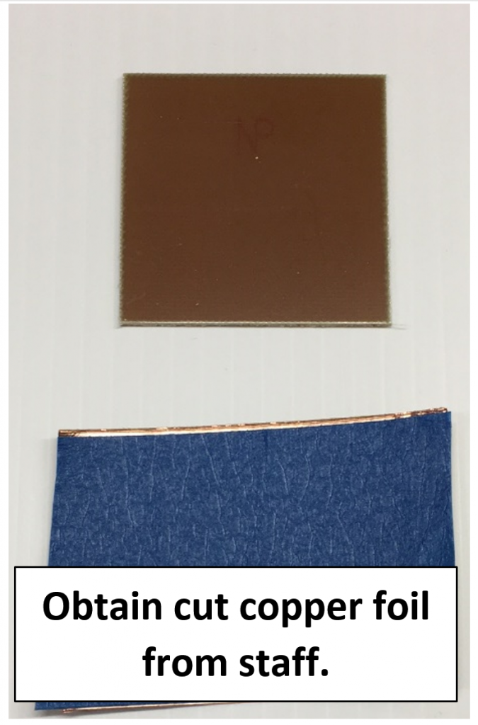
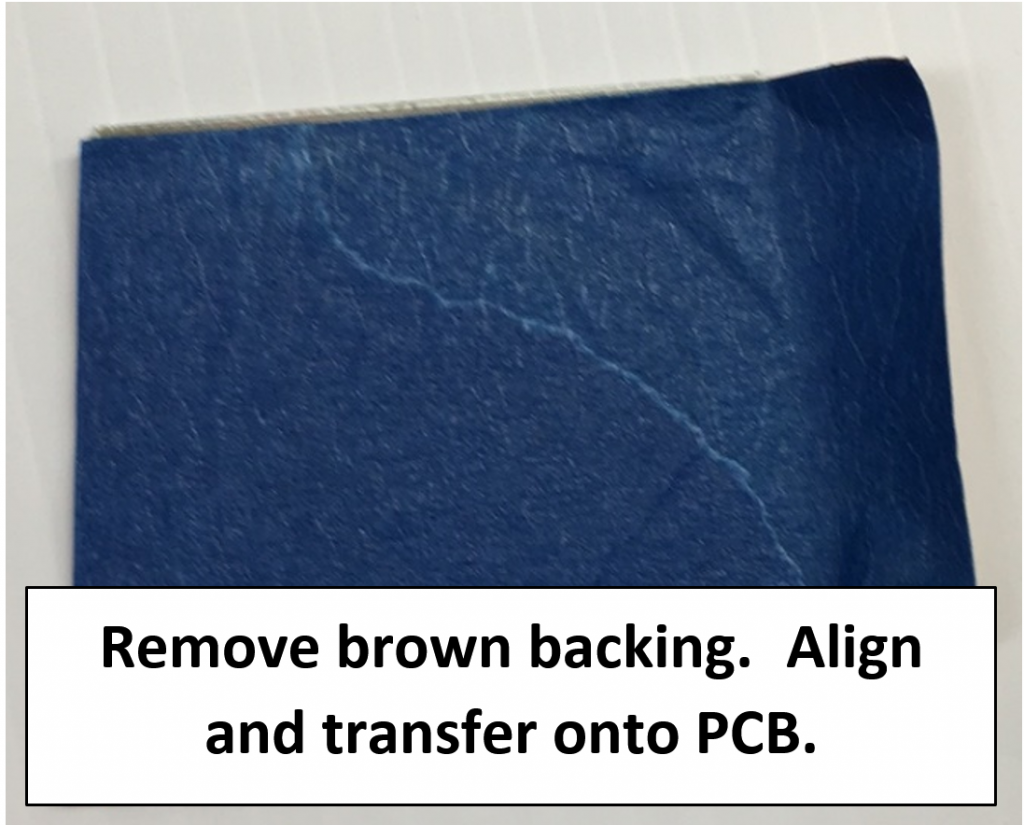
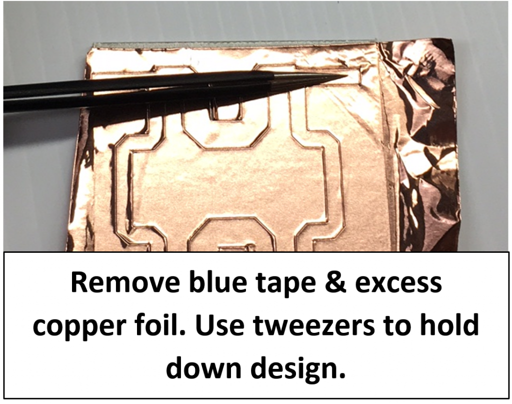
Assembly
You will transfer the cut design onto a PCB. The following images show the basic steps.
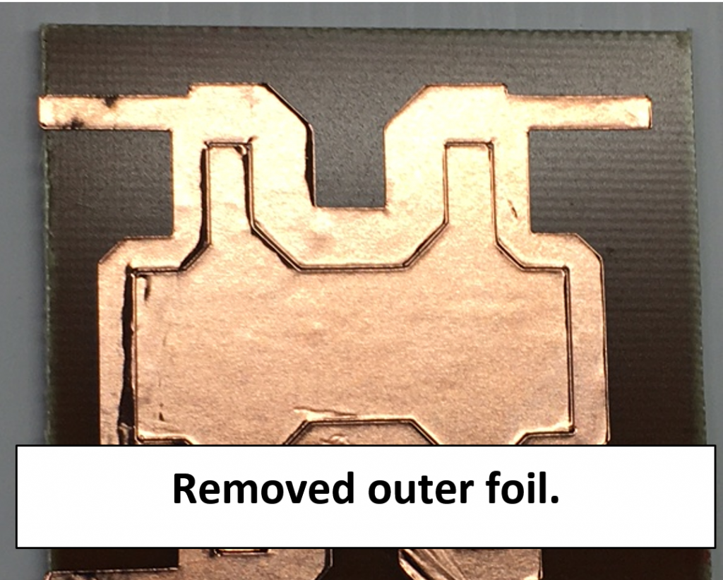
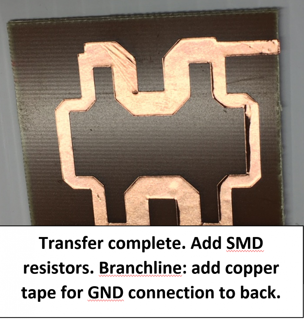
Solder SMA connectors to each transmission line (3). Break top PCB SMA legs off so that they do not interfere with the topside transmission line. For the 50 Ohm termination, solder it to the lower left trace and connect to the backside (GND) with the copper foil. Make sure to solder the copper foil to the backside also as the adhesive may not provide a good connection.
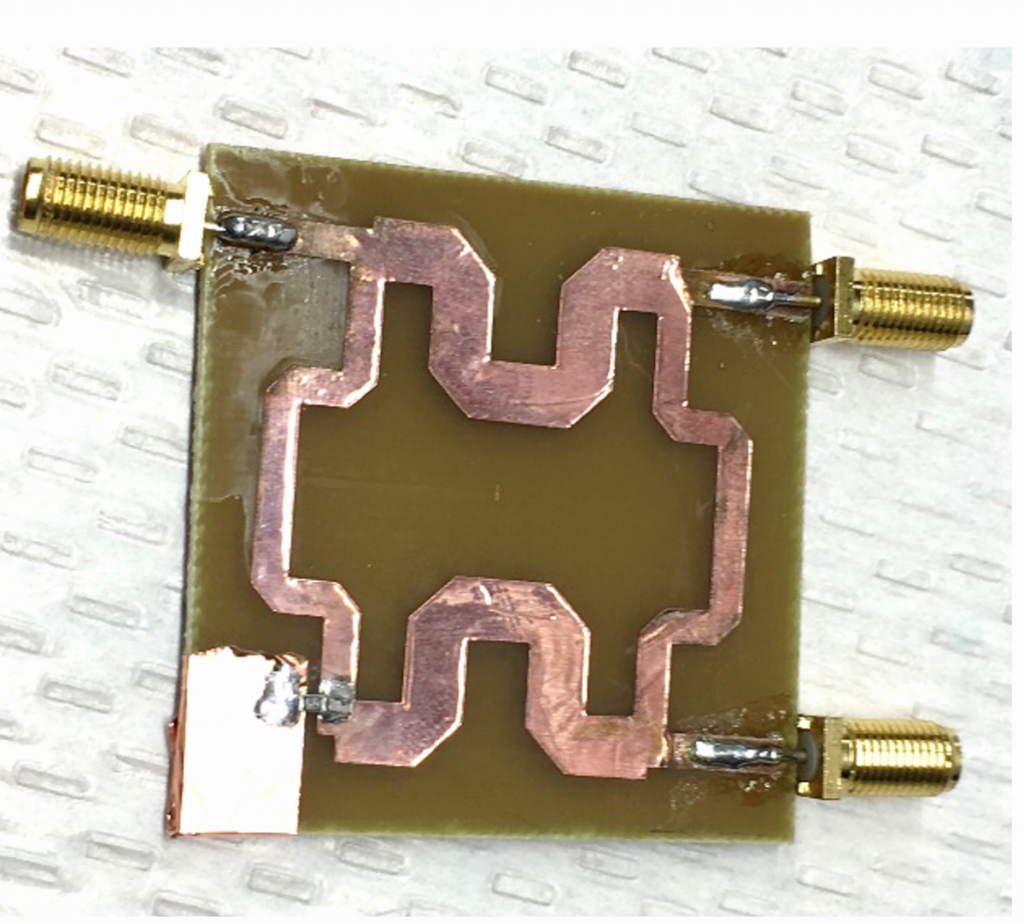
An image of a 2D cutter fabricated board is below.
Testing
The branchline is tested by connecting 2 of the three ports to the VNA and measuring S11 and S21 magnitude and phase.
Below are the two configurations for testing, note the 50 Ohm termination on the port without the cable. The left upper port connects to the Tx port of the VNA and the right cable (top or bottom) connects tot eh Rx port of the VNA.
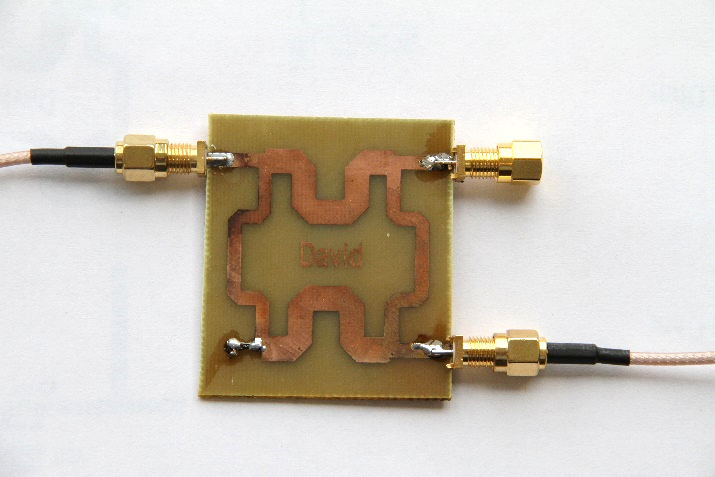
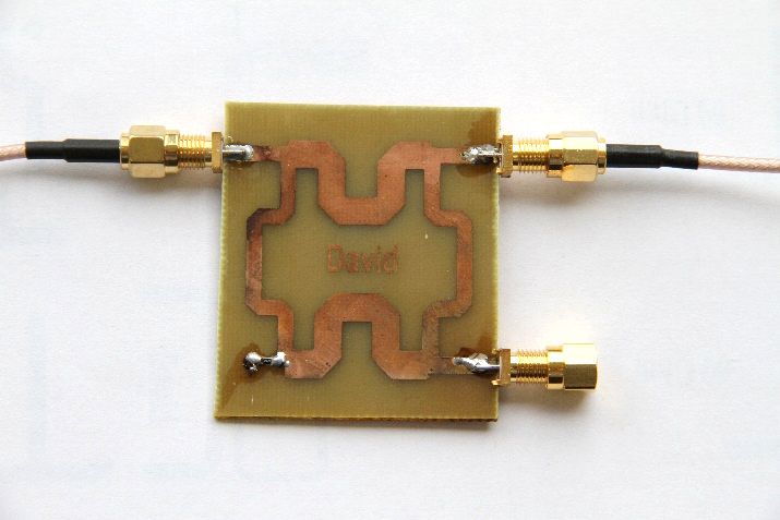
You can measure S11 to see the input impedance on the left port. You should then measure the phase on the right port bottom, then right port top. The difference in phase is the phase output, it should be close to 90 degrees. Below are the two measurements for the measurement of the bottom and top branchline ports.
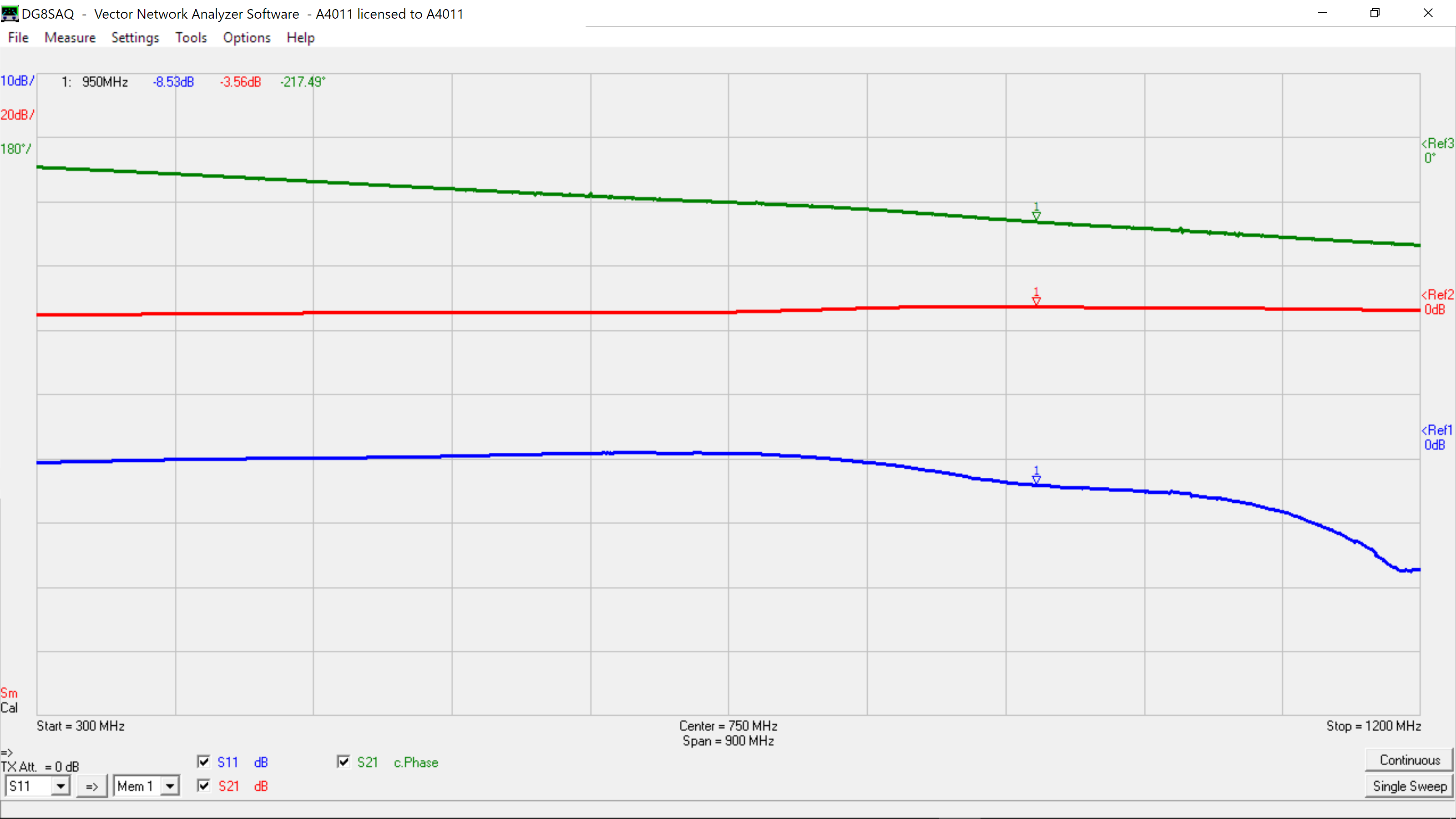
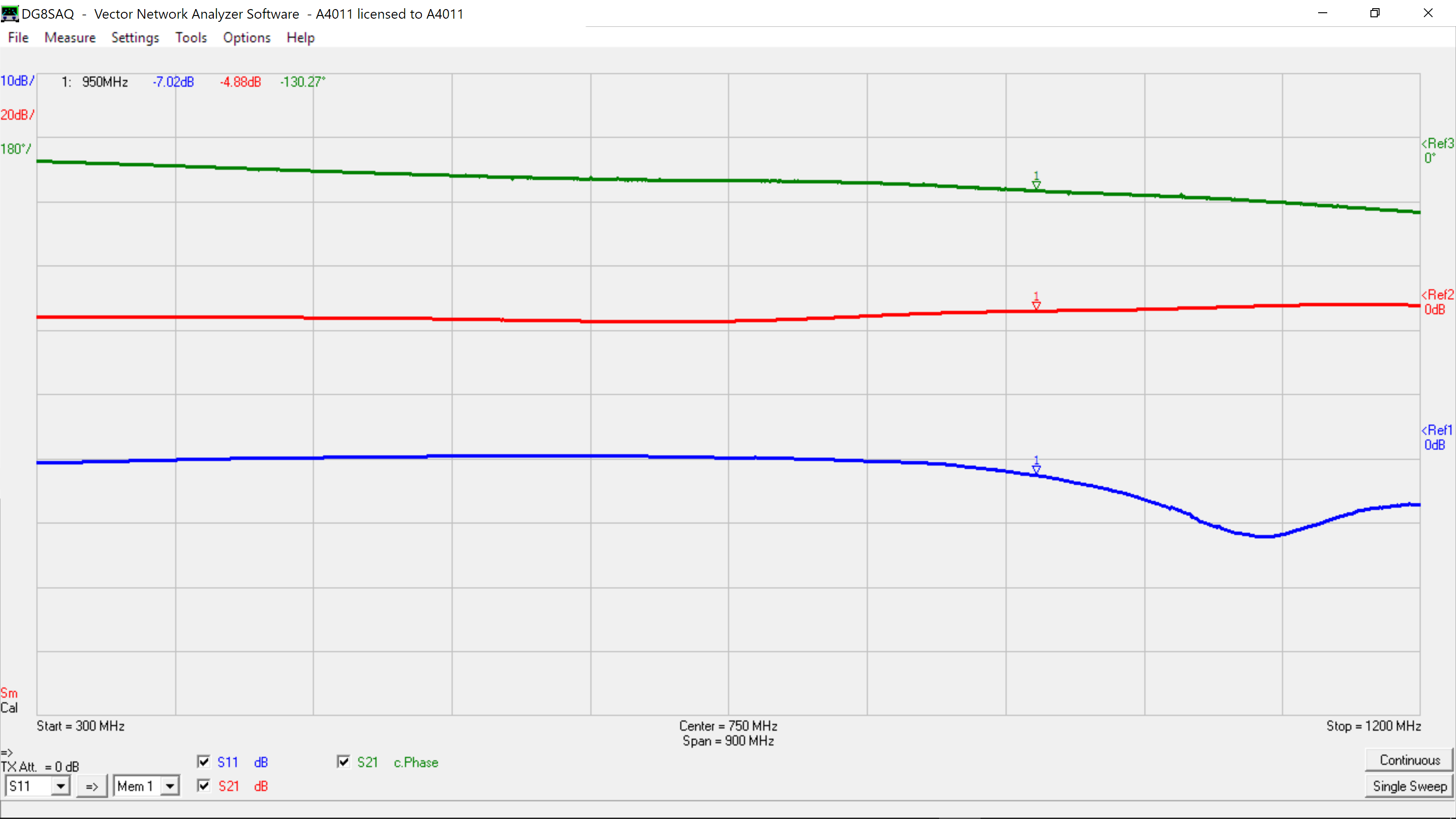
The phase difference is 217.5-130.3=87.2 degrees, which is a good quadrature separation. The loss however, is imbalanced, with one path having -4.88 dB and the other -3.56 dB. Ideal would be – 3dB in each leg.