Clapp Oscillator Theory
Theory of Operation
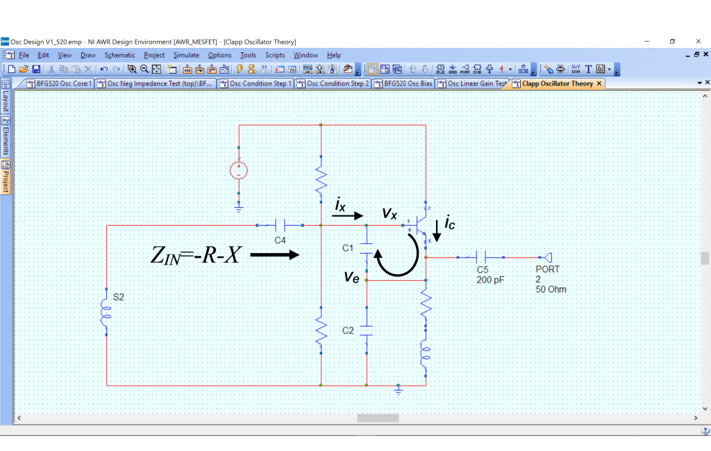
The Clapp oscillator is a negative impedance oscillator. Using capacitive feedback, we create a negative resistance (which is gain) at the base terminal of the BJT.
Let us assume the base current is negligible, therefore

Then the input impedance is

We see that the input impedance has a negative real part (-R) and that it is frequency dependent. It is also dependent on the values of the feedback capacitors. In addition, the input impedance has a capacitive component (-X).
To create an oscillator, we will cancel the capacitance of the input impedance at the desired frequency with an inductor:

The negative resistor, which is gain, will compensate for loss in the circuit.
Note: we require C2 and C1 to obtain the negative impedance
In our design, we will use simulation to evaluate the input capacitance and ensure the negative resistance. We will use an inductor to tune the oscillator to 950 Mhz.
Oscillator Core DC Bias
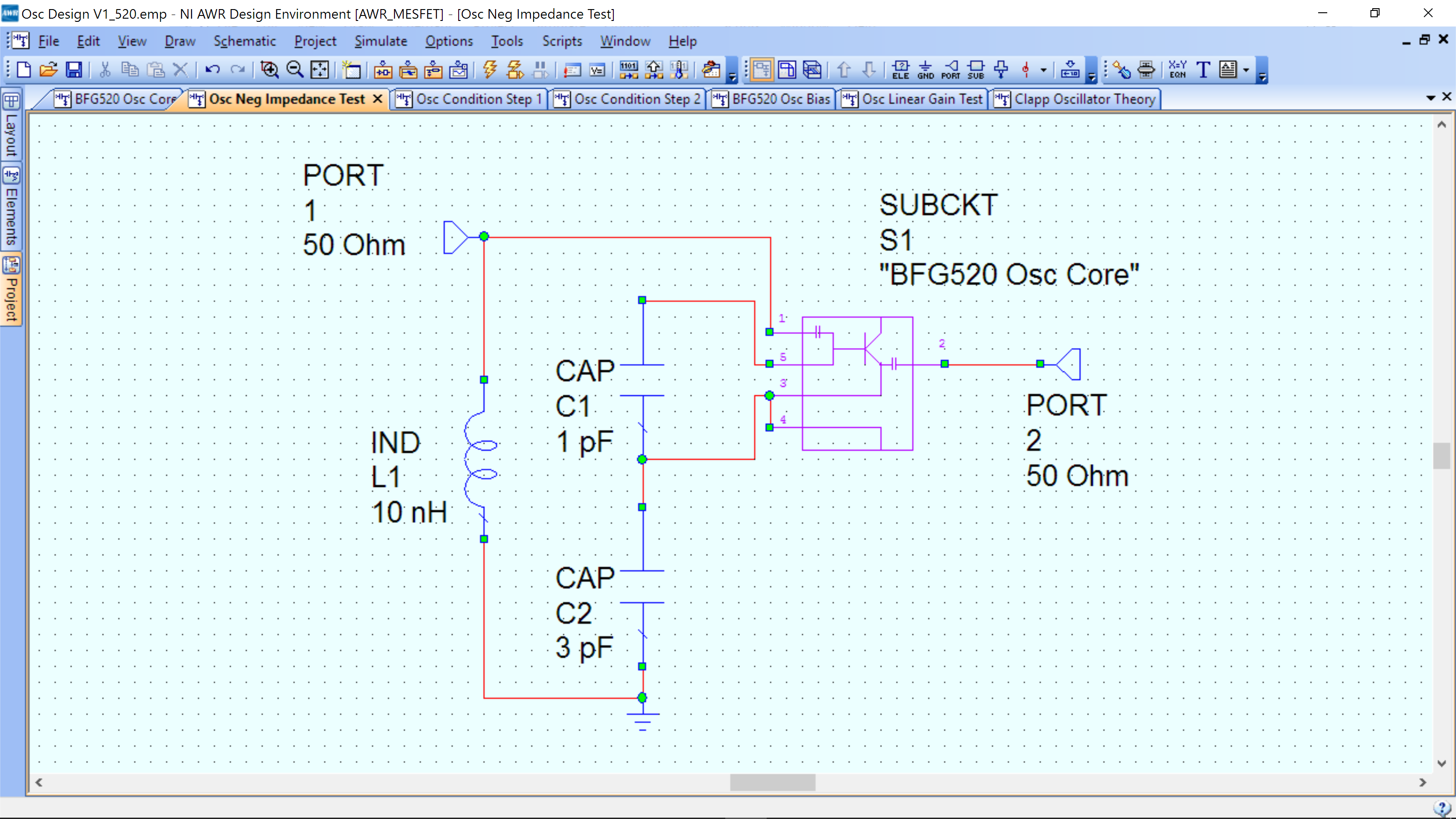
The basic oscillator schematic is shown below and can be found in the circuit design template as BFG520 Osc Core.
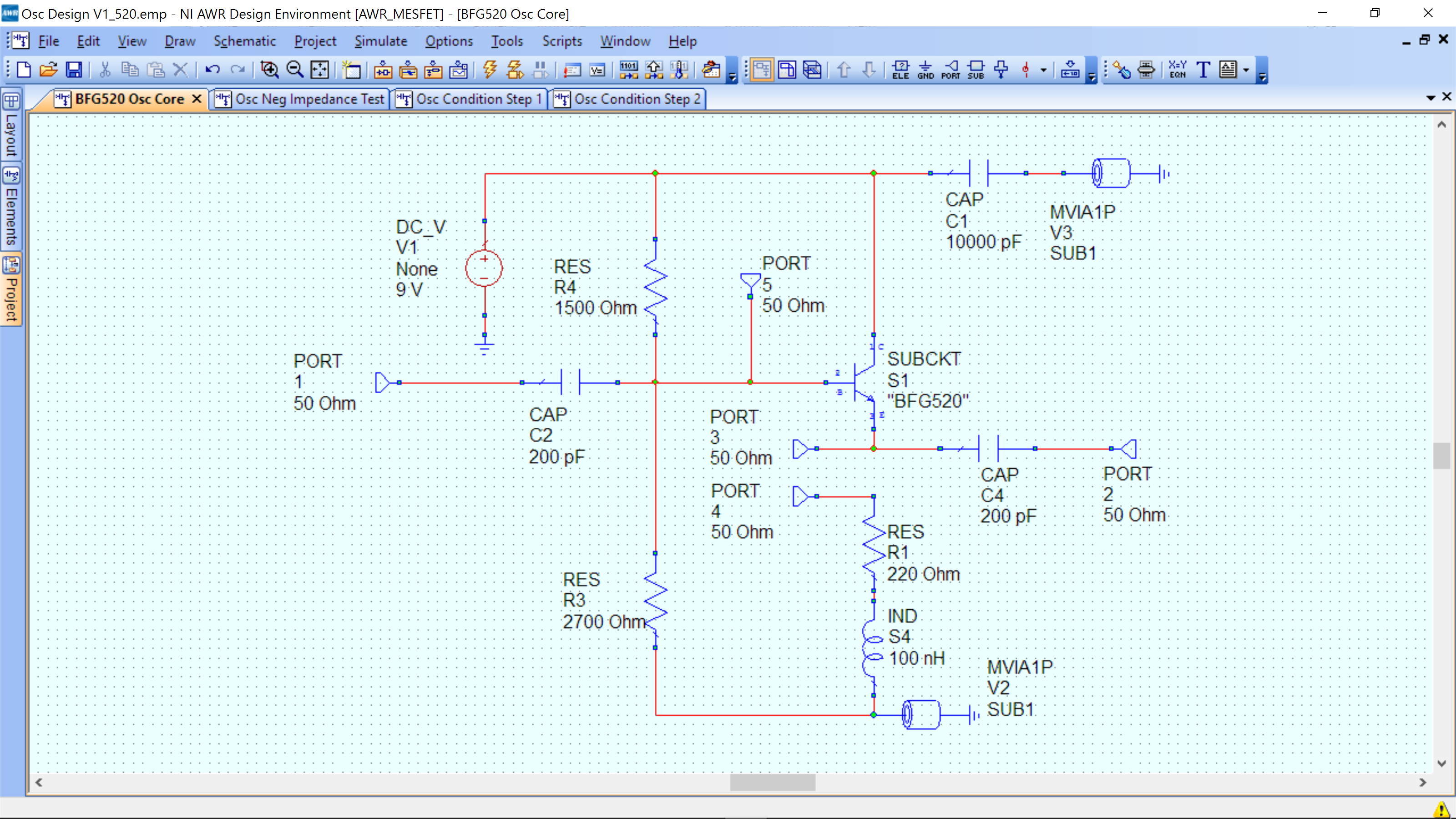
Component operation:
- R3, 4 – base bias voltage (and current)
- R1 – RF emitter load R93A BJT transistor
- S4 – Inductor – RF choke
- C2, C4 are DC blocking capacitors
- C1 is a supply decoupling capacitor. V2,3 are vias for our substrate.
- PORT 3,4 – break feedback look to allow us to test oscillation conditions
- PORT 5 – allows for feedback to create instability for oscillation
- PORT 1 – used for test analysis
- PORT 2 – output of oscillator.
The DC bias conditions for the oscillator core are shown below:
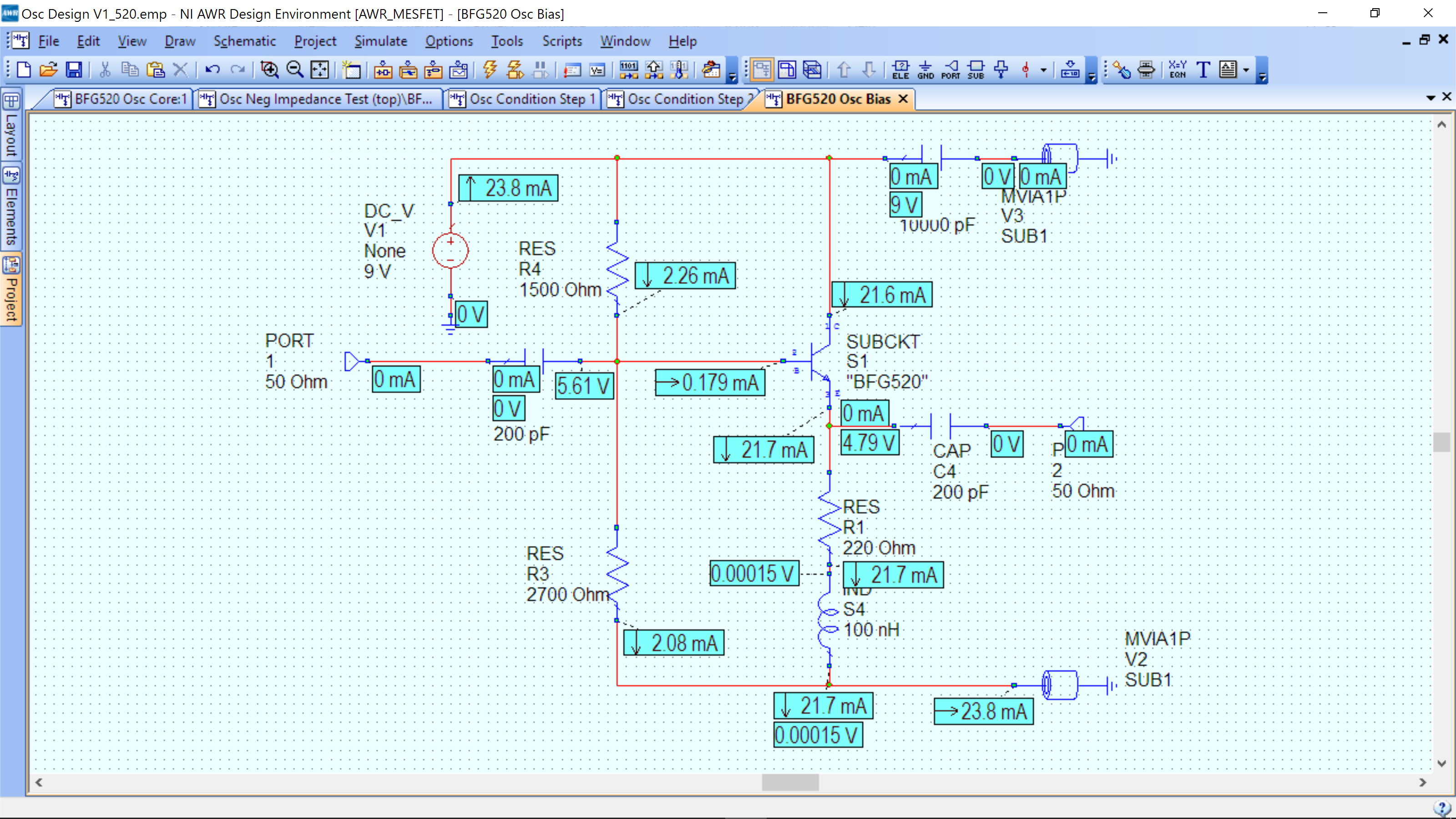
Note that the base voltage is 5.61V and the emitter is 4.79, with a 9V supply. You will use a 9V battery for your supply, which is usually higher than 9V, so the voltages you measure will be slightly different. These DC voltages will be a guide to checking the DC bias of the core after assembly.
Oscillator Core AC Gain
The first step is to measure the gain of the oscillator core.
Create a new schematic, Project -> Add Schematic.
Insert the oscillator core by copying it from the “Components for design” schematic. Make sure it is enabled (right mouse click, then enable). The components on the design schematic are by default disabled (grayed out).
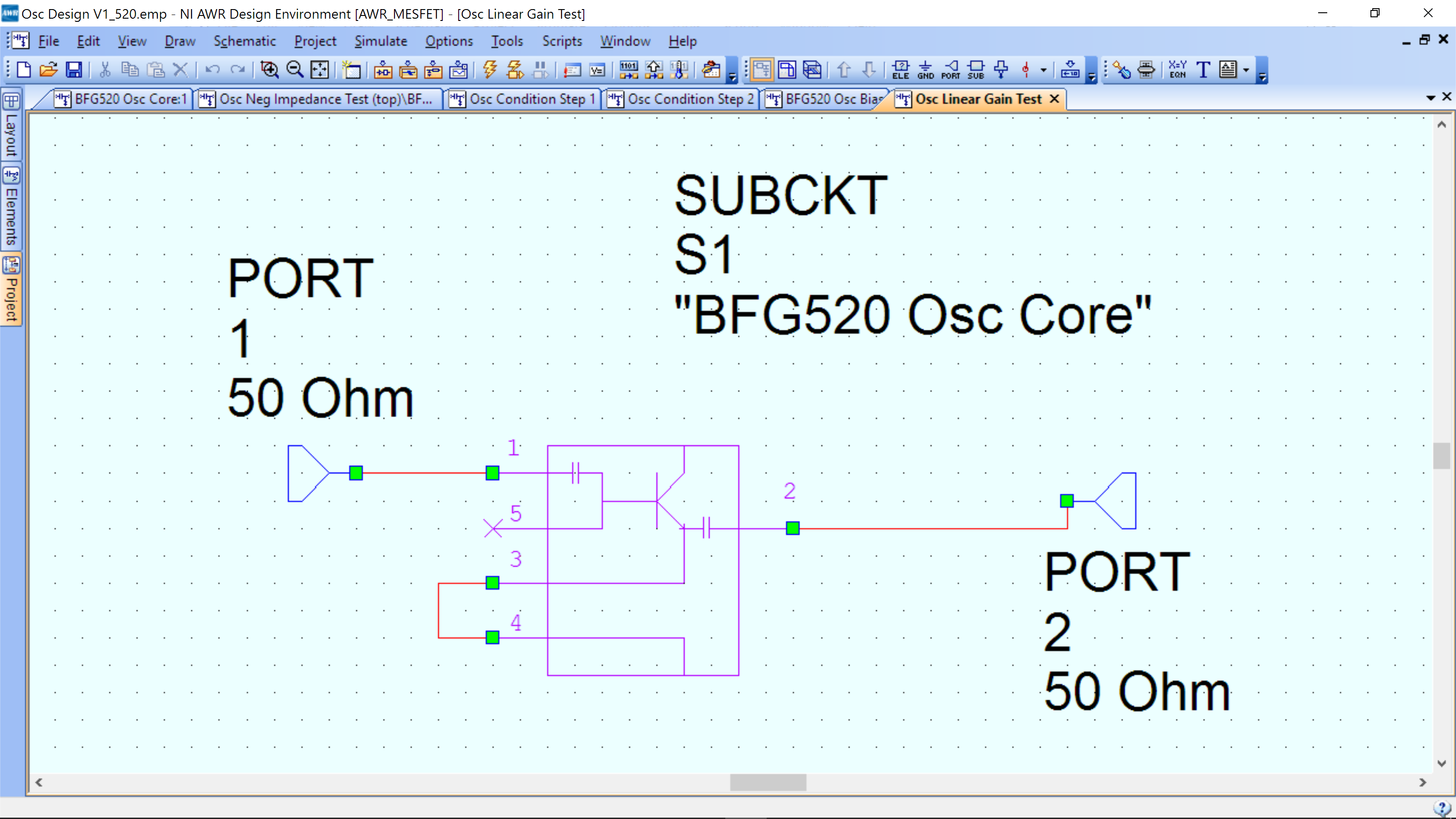
Configure as below, noting we are shorting two pins (just connects the emitter to the bottom pin of the symbol – pins 3 and 4of BJT) and leaving one port, pin 5, open (no feedback).
Components can be added as follows:
- PORT and GND can be added directly from the tool bar at the top of the software (labeled “PORT” and “GND”)
- All other elements can be added by Ctrl+L then type the name of the element, e.g. RES or CAP, and you will find it in the list that appears.
- Special components: BFG520 Osc Core, OSCTEST and OSCAPROBE, MVIA1P (special via to ground) must be copied from the Design for Components Schematic in the template provided.
Setup the simulation by going to Options->Project Options->Frequencies and setting the range from 0.5 to 2 GHz in 0.01Ghz steps. Hit Apply and make sure replace is selected.
The measure the gain (S21), both in magnitude and phase. Click Project->Add Graph. Name is something useful, e.g. Osc Core Linear Gain, and make sure Rectangular is selected for the plot type. Once the graph is created, Right Mouse Click->Add New Measurement. The following window will appear:
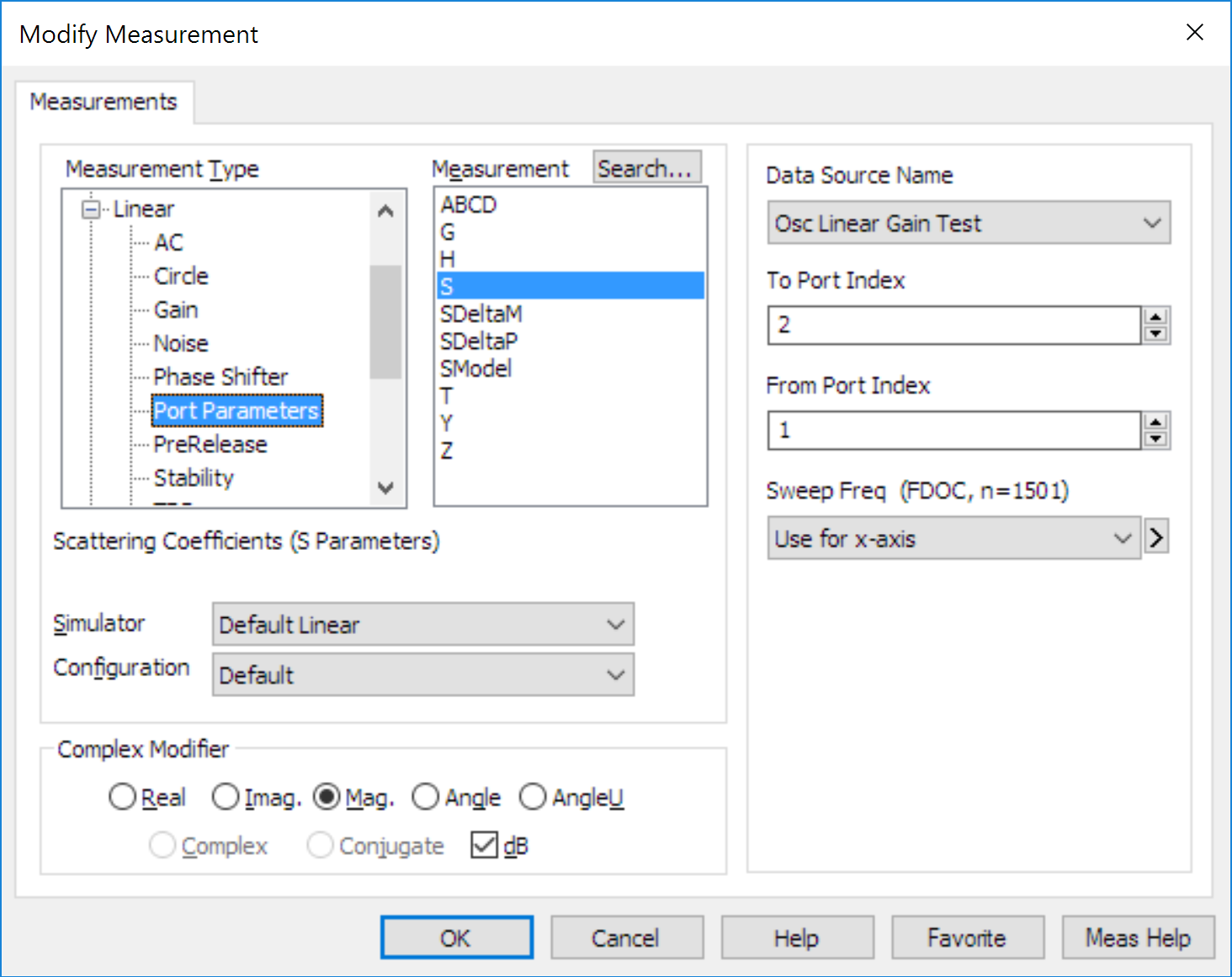
Ensure that the Data Source Name is the design you want (not All Sources), then select Port Parameters->S then select 2 and 1 from the port indices. Select Mag and dB. Hit Apply. Do the same, but for Angle (deselect dB). The results are below. You can add a marker by Right Mouse Click->Add Marker.
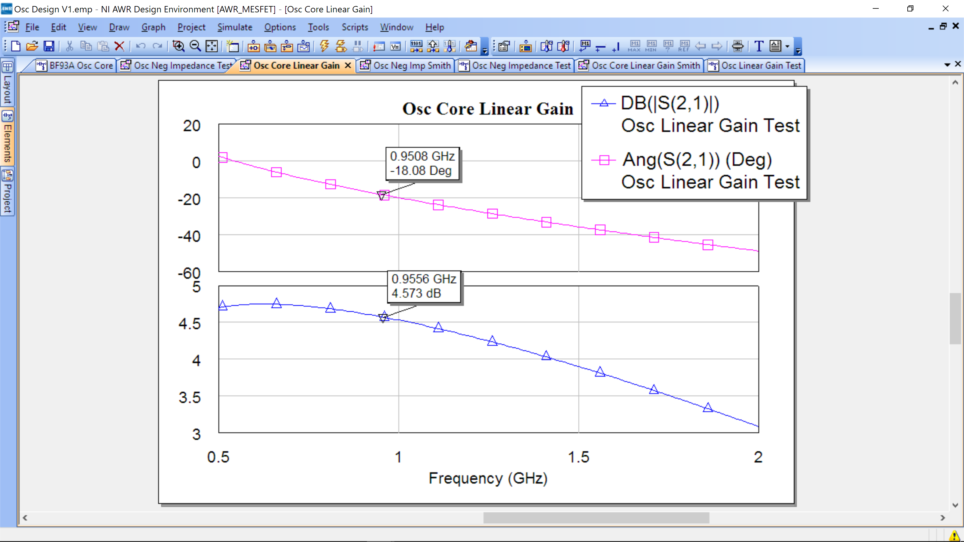
The amplifier has a gain of 4.5 dB at 950 Mhz, and a phase shift of 18 degrees. We also measure the input impedance for contrast later in the design. The Smith chart is shown below. To graph a Smith chart, Project->Add Graph then select Smith Chart as type. You can add then add the impedance as before, selecting Complex.
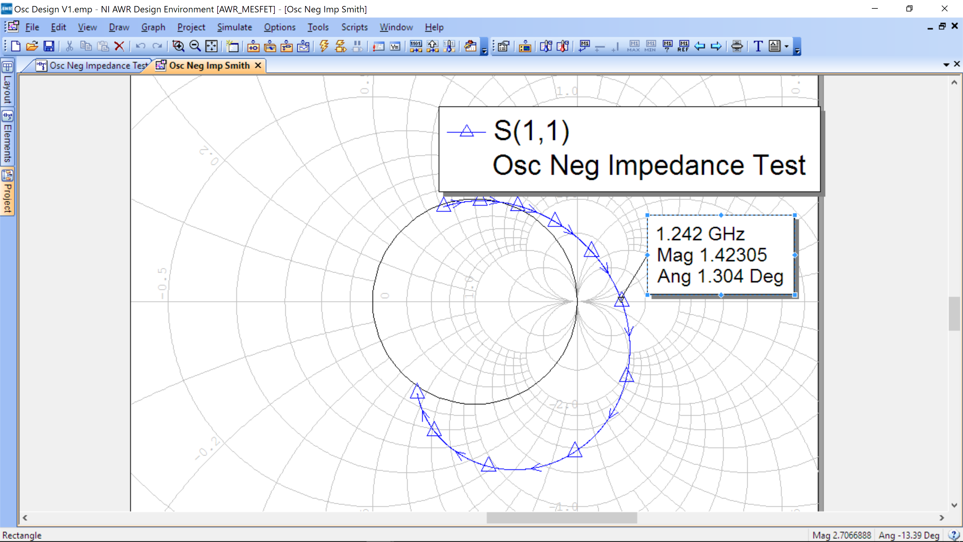
The resulting S11 is:
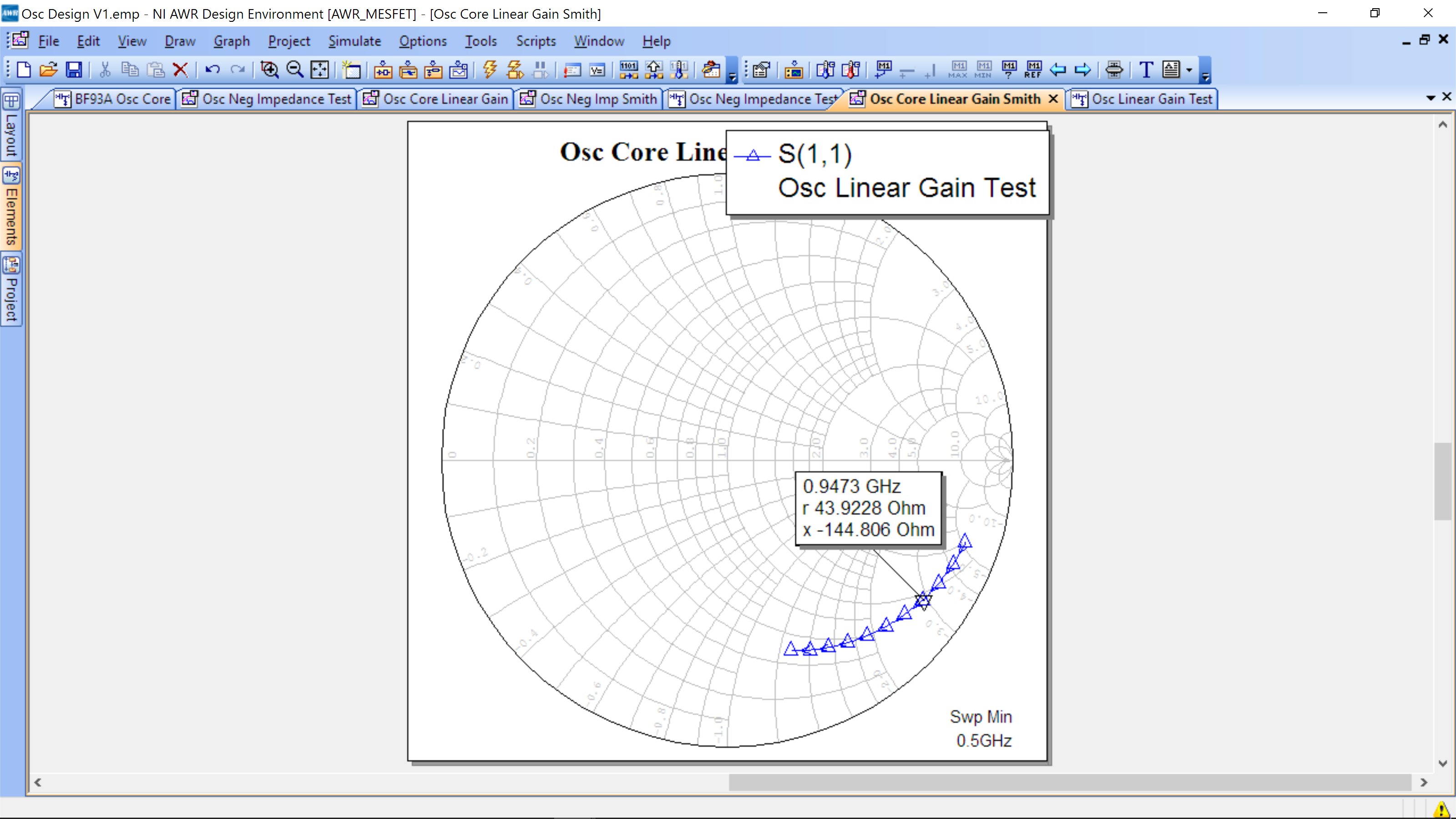
The input impedance is 43.9-144j Ohms and with Gamma = .84 (not shown, but can be seen by double clicking on label and choosing reflection coefficient instead of impedance).
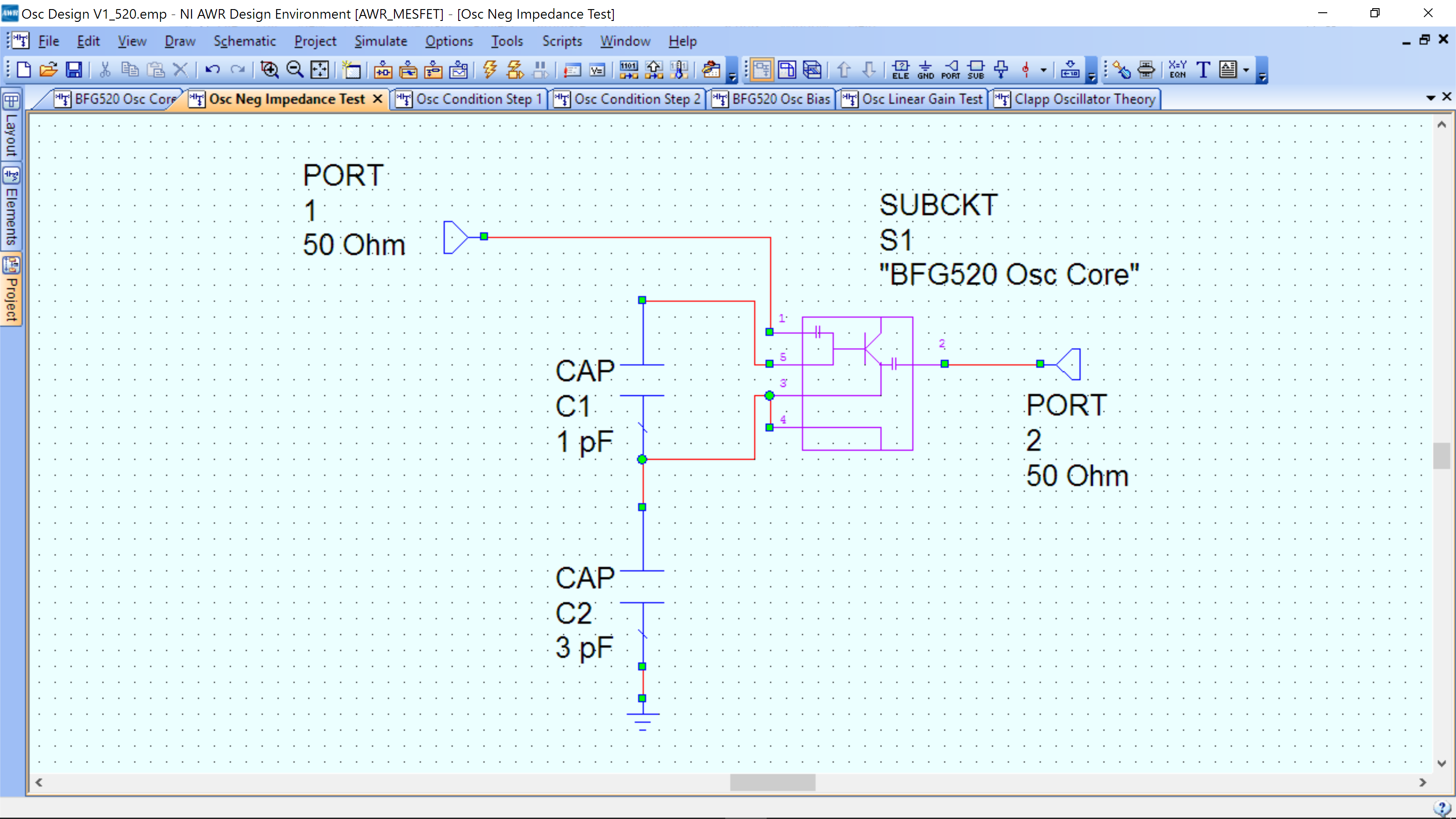
Negative feedback
To build an oscillator, we will introduce feedback by connecting a capacitor to the base and emitter and emitter and ground.
We recommend copying each schematic to a new one for each section. This can be done through the project tab on the left. Project then find the schematic you wish to copy. Right Mouse Click->Duplicate. Then on the copy, Right-Mouse Click->Rename and enter the new name of your schematic. Do this for each section (as it will then keep copies of each step of the design process).
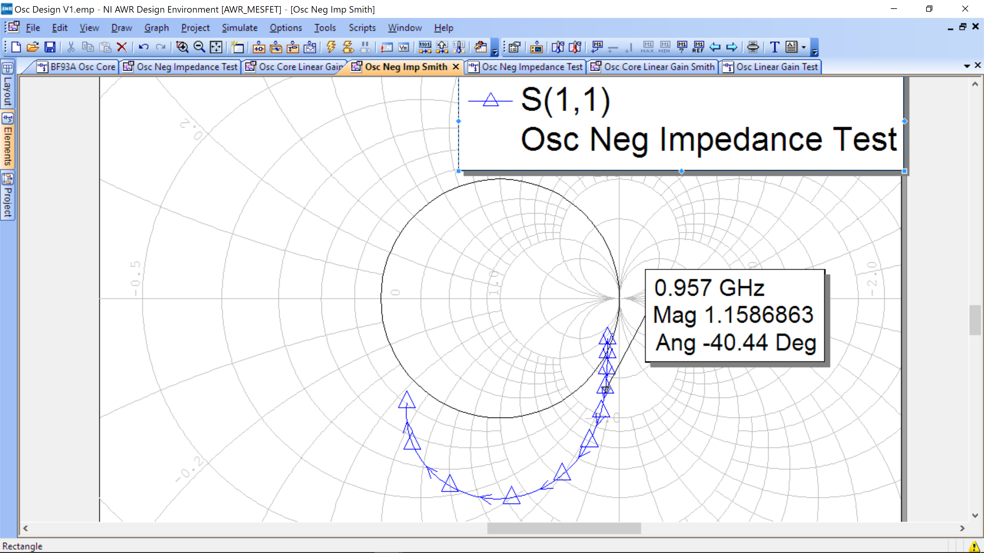
Capacitor C2 can be changed to modify the feedback loop gain. We now remeasured S11 and see that it is greater than 1. This can be intuitively understood as gain, as Gamma is the reflected/incident. A value greater than 1 means you get a larger voltage reflected than was incident, indicating amplification.
This can also be plotted on a rectangular plot
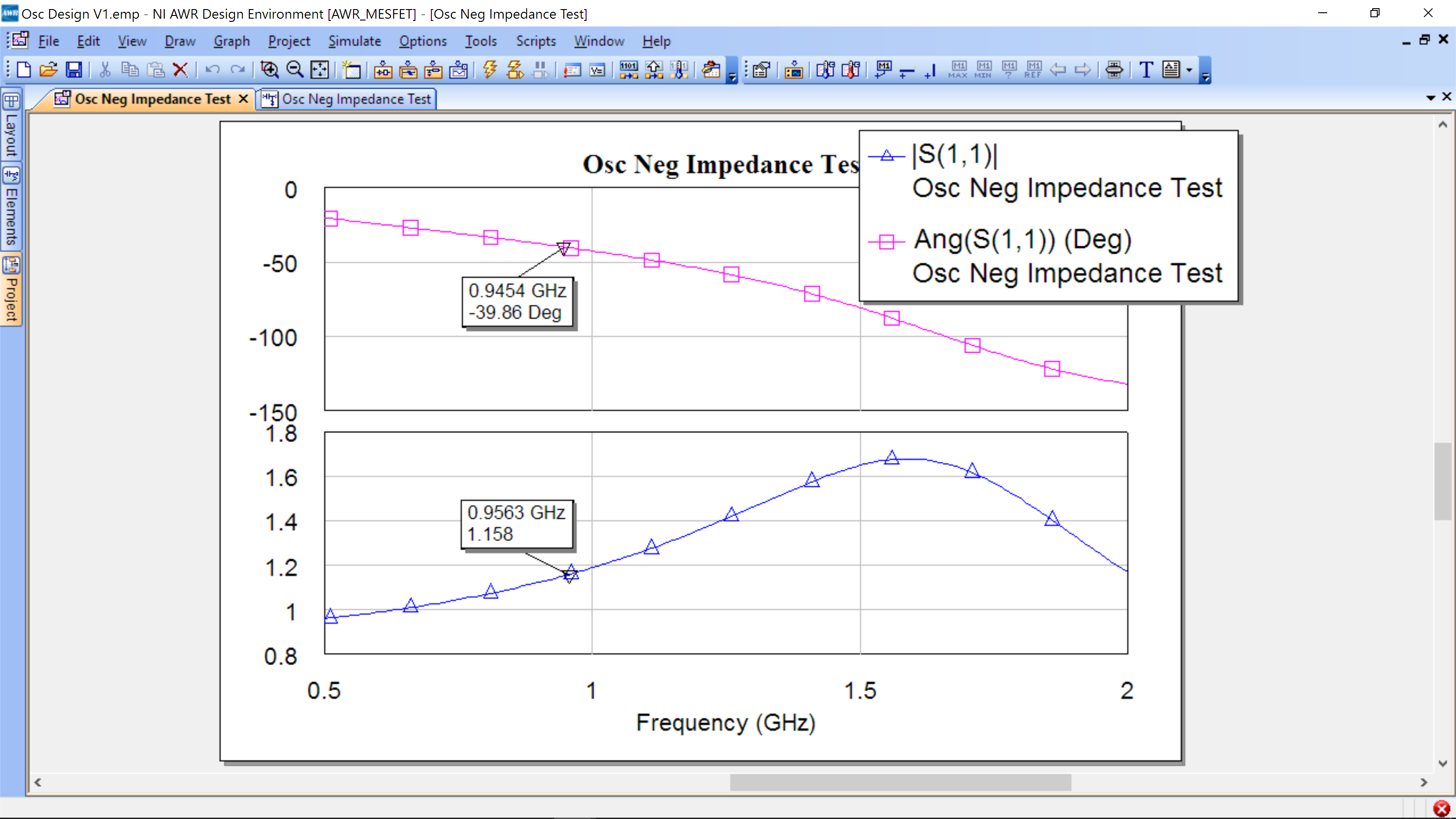
By changing C2 to 5 pf the gain is increased.
You should also note that the input is highly capacitive (seen by the S11 in the lower part of the Smith Chart and that the angle/phase is negative.) This is expected from the theory section.
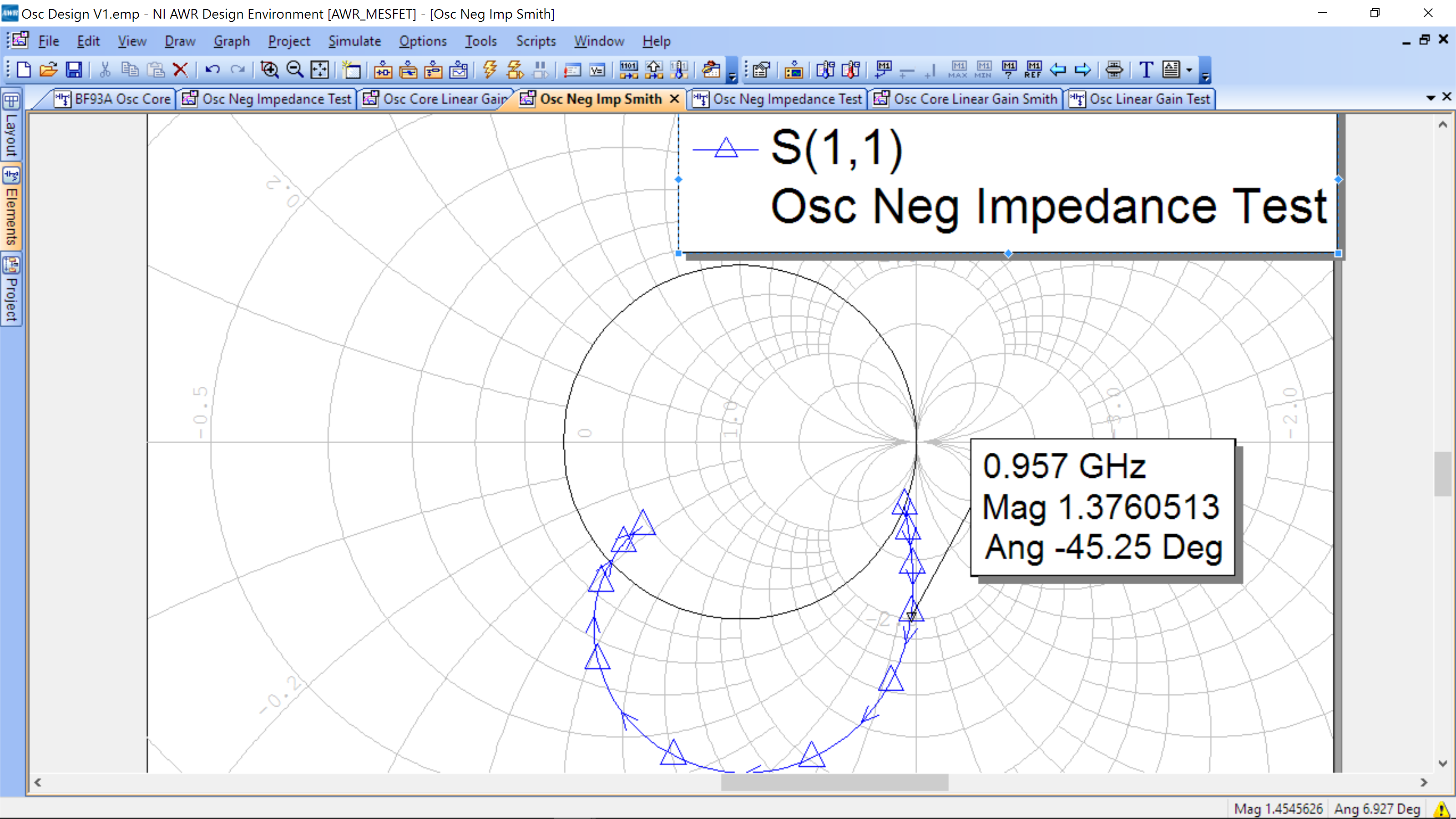
To oscillate, we need the phase shift to be canceled and Gamma still greater than 1 (gain). Temporarily place an inductor in series with PORT 1. Set the value to 10 nH.
The reflection rotates counter clockwise.
This will get you close to the oscillating condition and we will move to the next step.
Oscillation Step 1
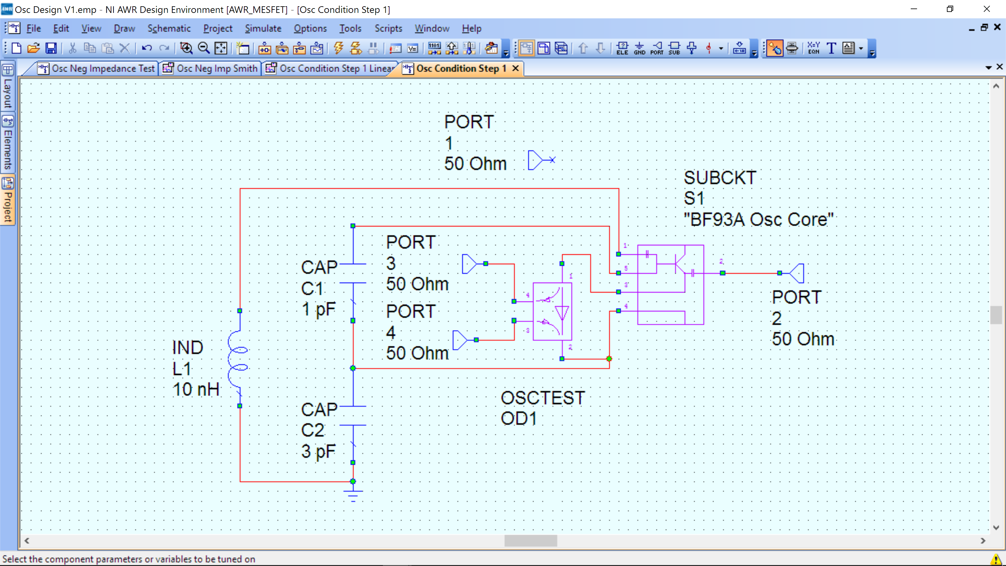
To measure the oscillation conditions, we want to close the feedback loop and see how a small test signal propagates around the loop. Duplicate and Rename your previous schematic for this section AWR has this built in through OSCTEST.
We have provided an OSCTEST in the Component Design schematic that you can copy and paste (do not add OSCTEST as an element yourself – make sure to copy and paste). Make sure it is enabled when you insert it in your oscillator schematic. It should look like the image below.
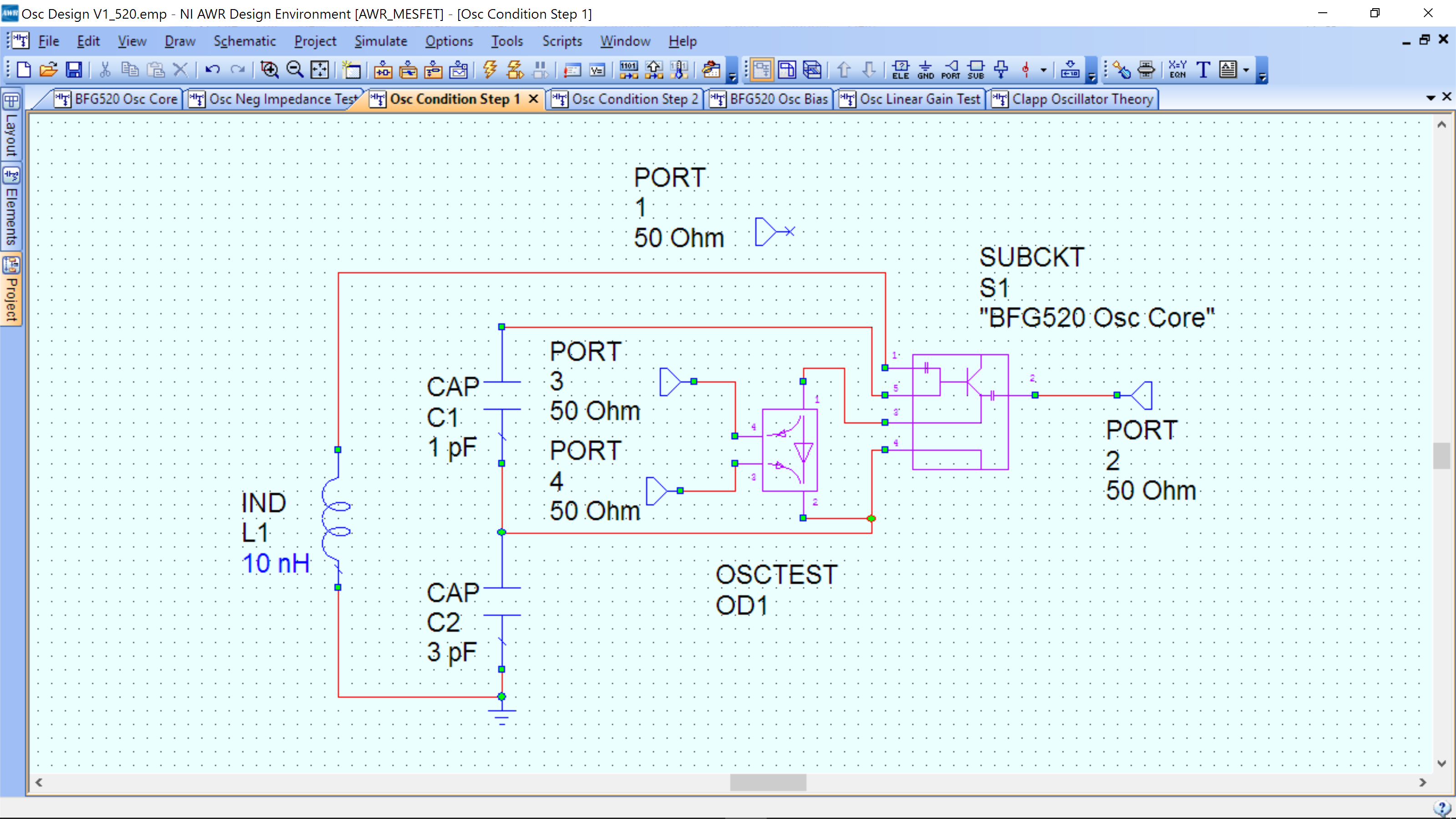
Note we have disconnected PORT1 as it would load the oscillator. OSCTEST sends a small signal into the loop and looks for the amplitude and phase of that signal when it returns. Calculating the loop gain and phase. For oscillation, the phase should be zero and the gain > 1 (or > 0 dB). The phase condition is ensure the signal out of the BJT matches phase with the stimulus (0 degrees) for positive feedback.
You can now measure S34, both amplitude and phase. Note it is S34, as we want what comes out of PORT3 from what goes into PORT4.
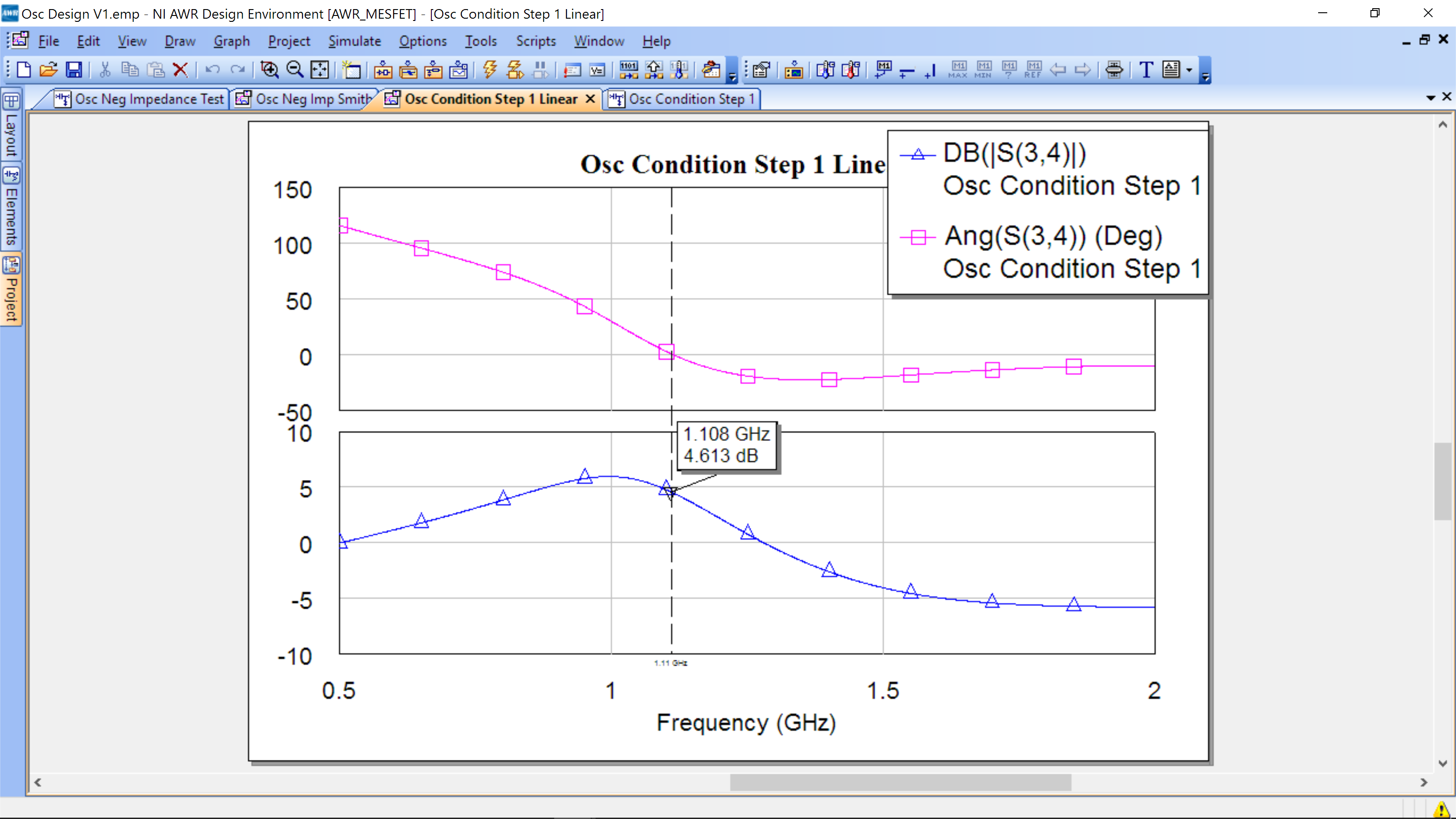
We can see that the phase and gain condition is met at 1.108 GHz. Click on the schematic, then screwdriver on the upper right:
Then click on the inductor value (10 nH). It will turn blue, and now you can use the tuner (next to where you found the screwdriver) to adjust the inductor value. Simply click on the tuner button, then adjust the slider so that the phase and gain are met at 950 Mhz.
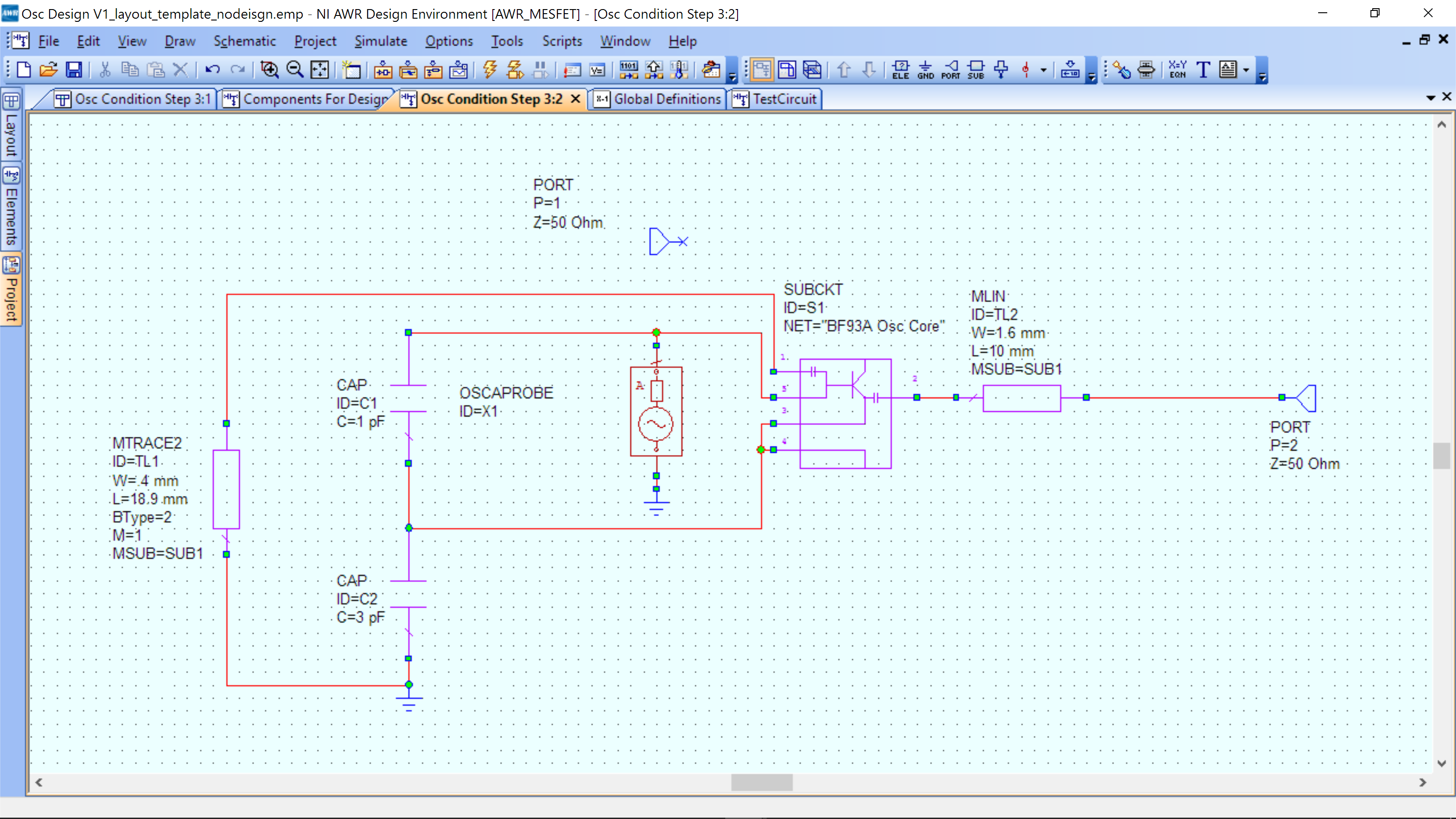
Oscillation Step 2
Now that the small signal parameters are set, we want to examine the large signal oscillation. Duplicate and Rename your previous schematic for this section. In this section we remove OSCTEST and insert OSCAPROBE. Please copy and paste form the Components for Design schematic (to ensure parameters are set correctly. Do not insert as a new element).
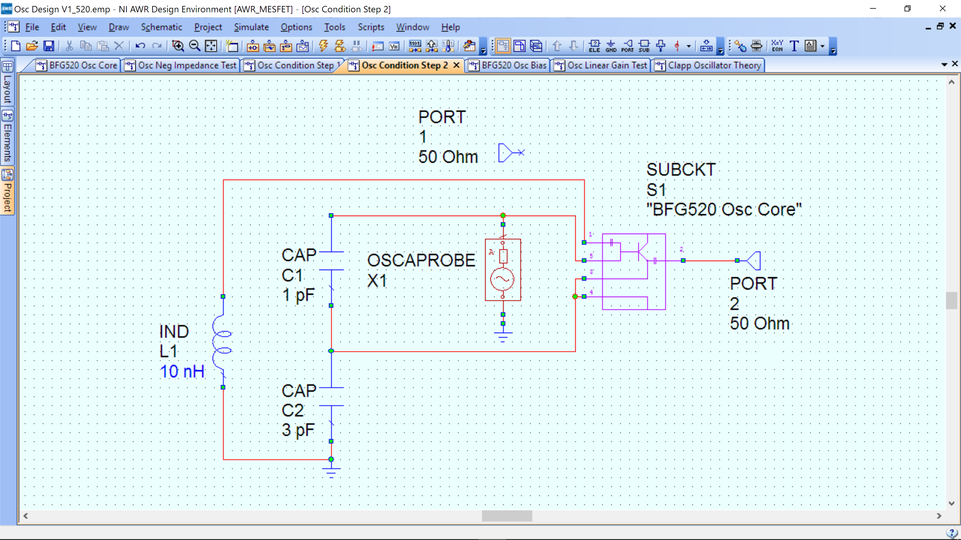
Now Project->Add Graph.
Then Add Measurement -> Nonlinear->Vtime and select PORT2.
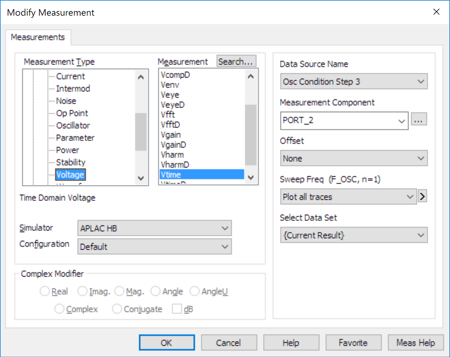
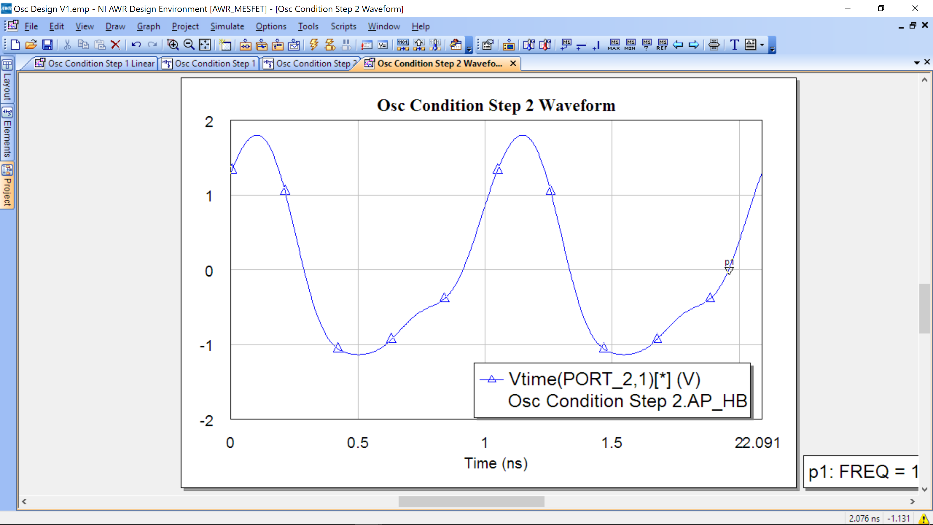
This will run the harmonic balance simulator to solve for the time domain waveform. The following is the waveform:

It shows exactly two periods, so the frequency can be calculated from the number on the right. In the example above, it is 893 MHz. The inductor can be tuned again until the desired period of 1.05ns is achieved (or 2.1 ns for two periods). Rerun the simulation once you have it close to your goal so that you get an accurate simulation.
Oscillation Step 3
We do not have a wide selection of inductors and, with parasitics, it is not likely your original value will yield the exact oscillation frequency. We will therefore synthesize an inductor from a microstrip and lay it out so that it will can be tuned by moving a small short across the microstrip.
Create a new schematic. Project->New Schematic.
An inductor has a positive reactance with (ideally) no real component. We will create this with a thin microstrip. Insert a MLIN with a width of 0.4 mm and an inductor with the value you have designed (we show 10 nH below for example). The substrate definitions are in the circuit template, so nothing has to be adjusted or entered for your design.
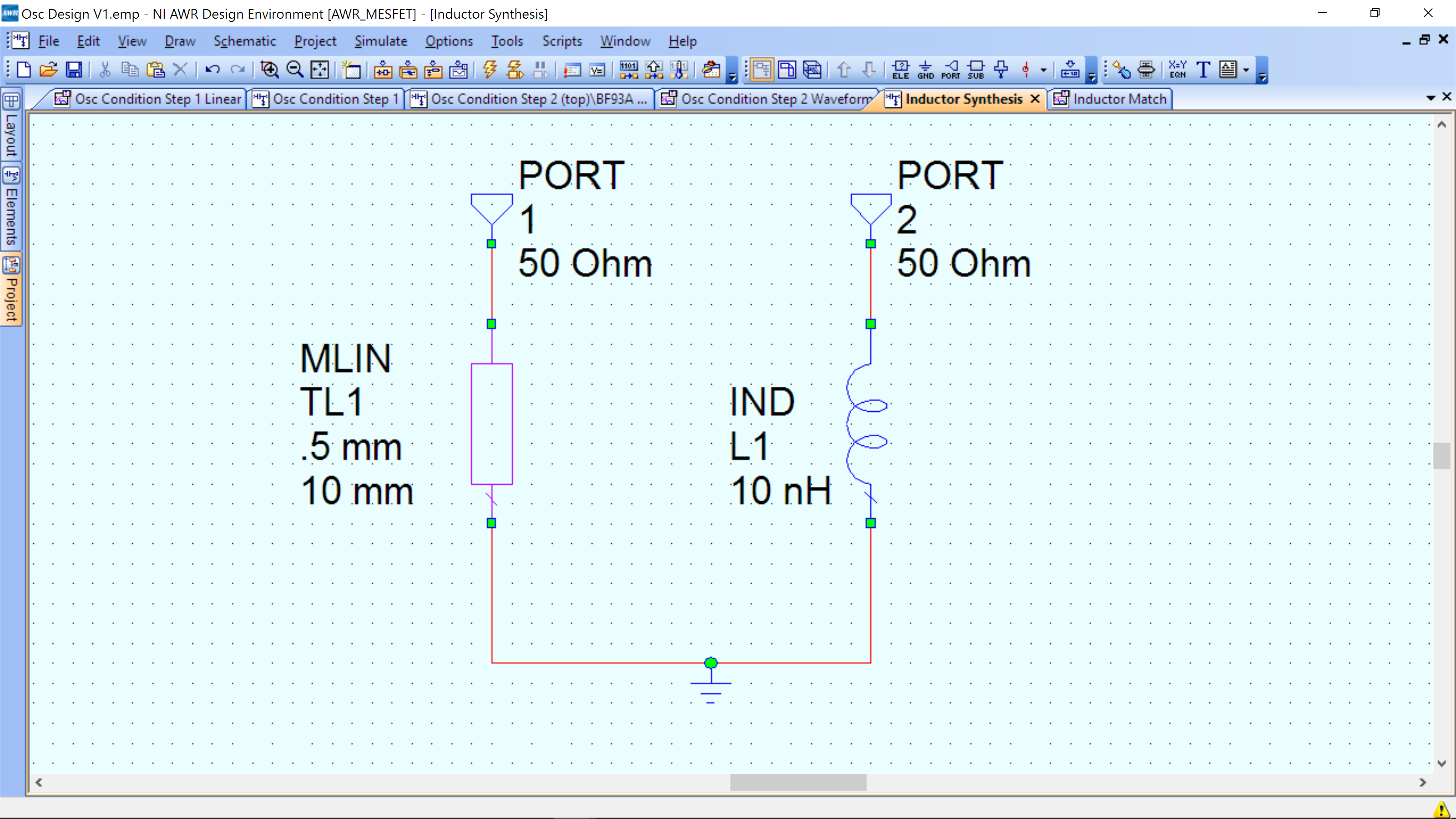
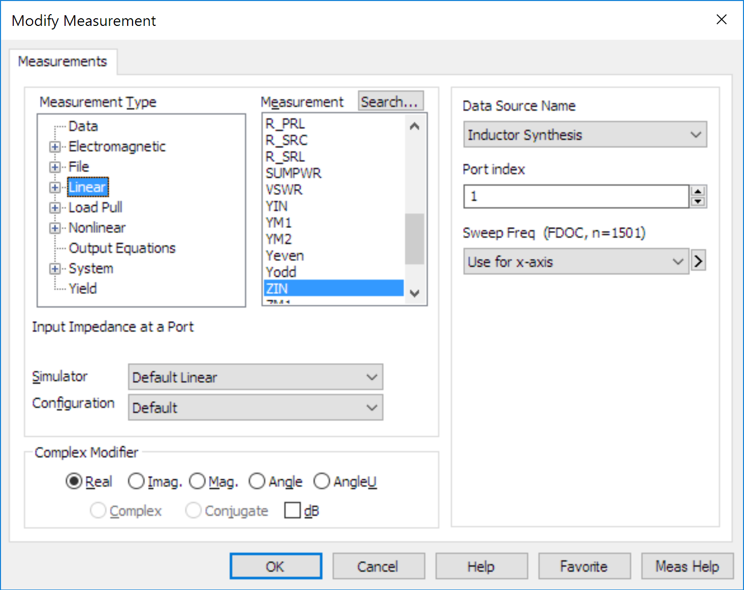
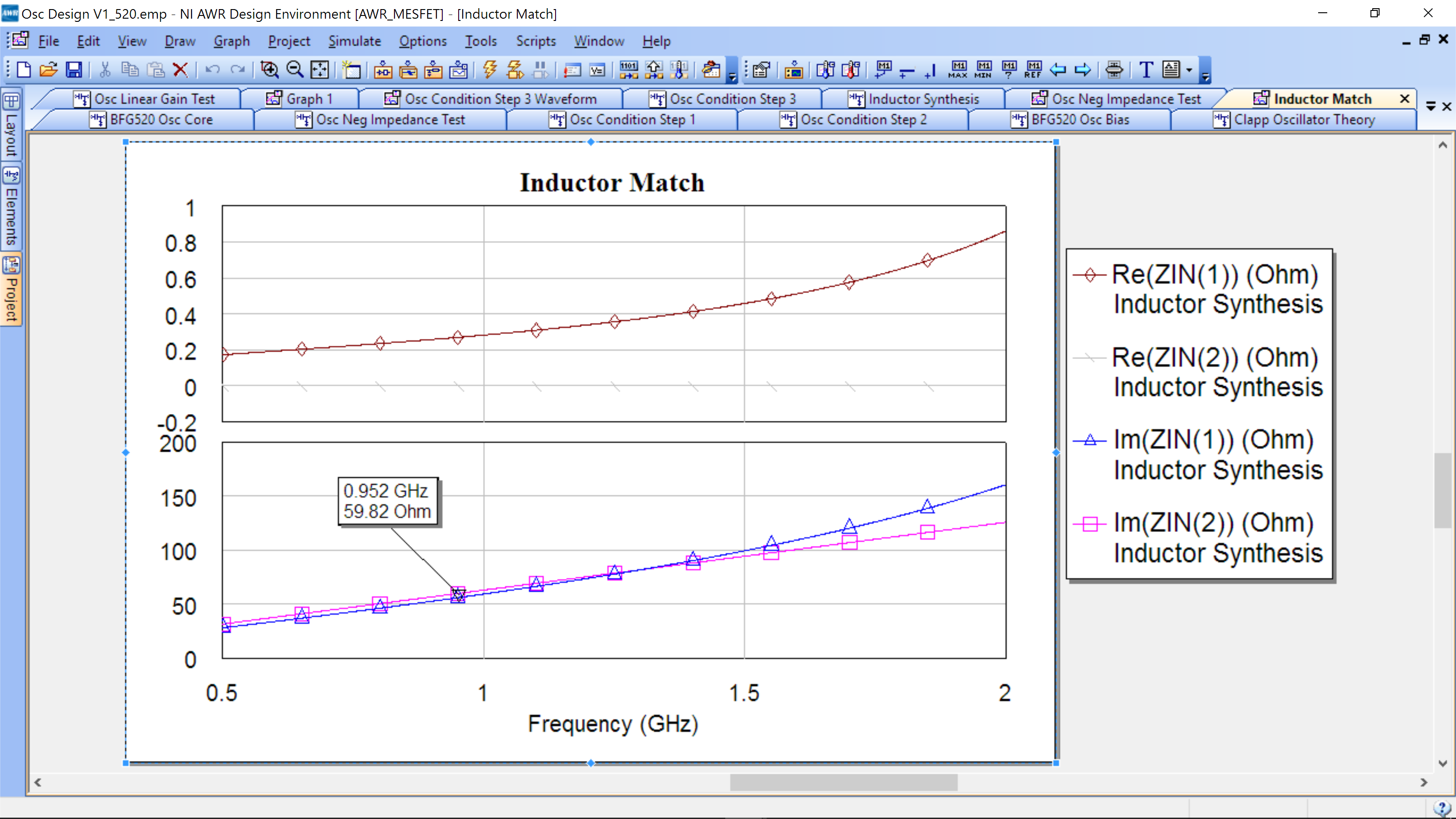
You can measure input impedance directly: Project->Add Graph->Rectangular. Then add measurement Linear->Zin. Then select real and imaginary.
Below is the simulation result from an example solution.
Now that we have an equivalent inductor, we can start layout.
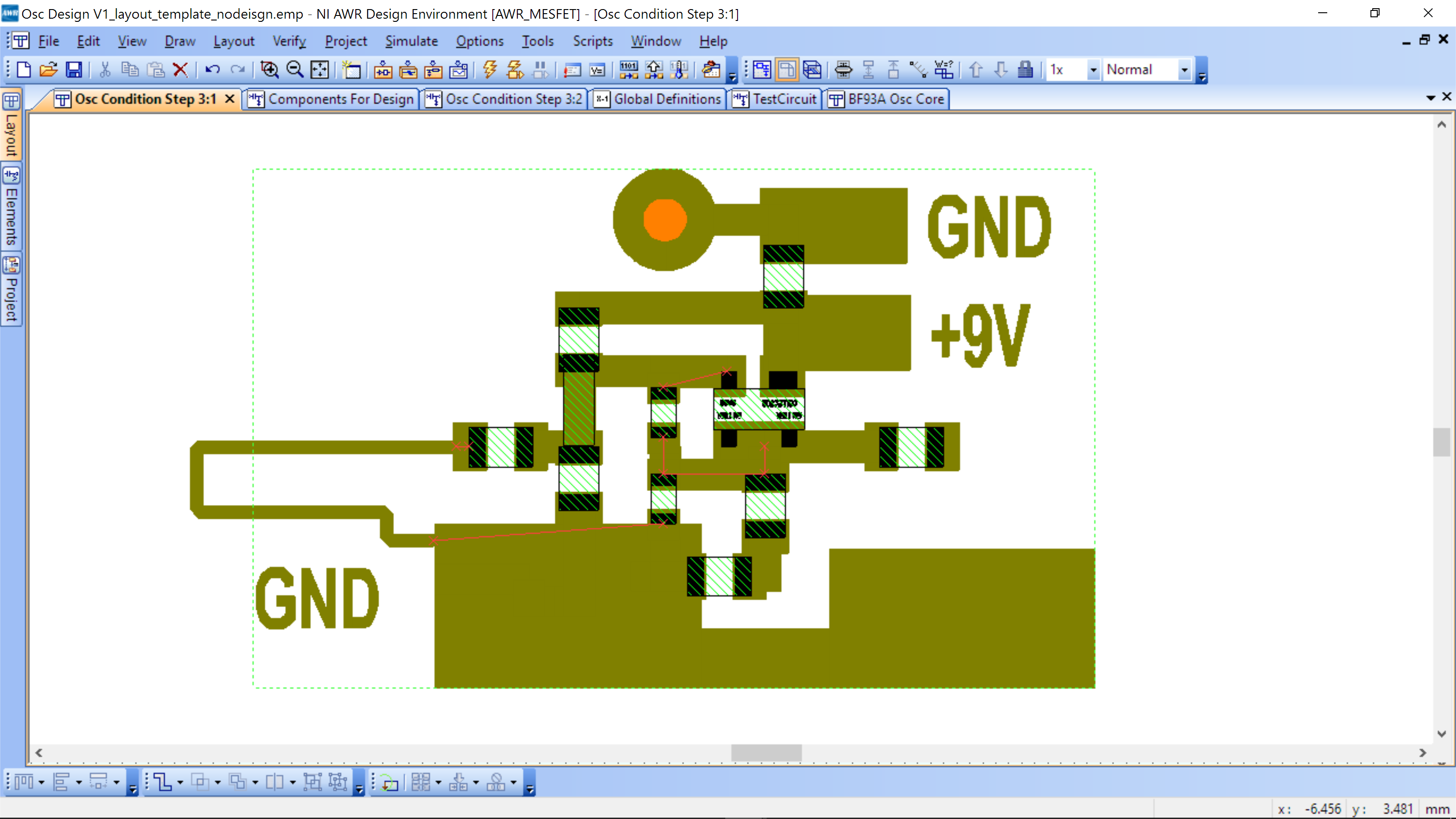
Oscillation Layout
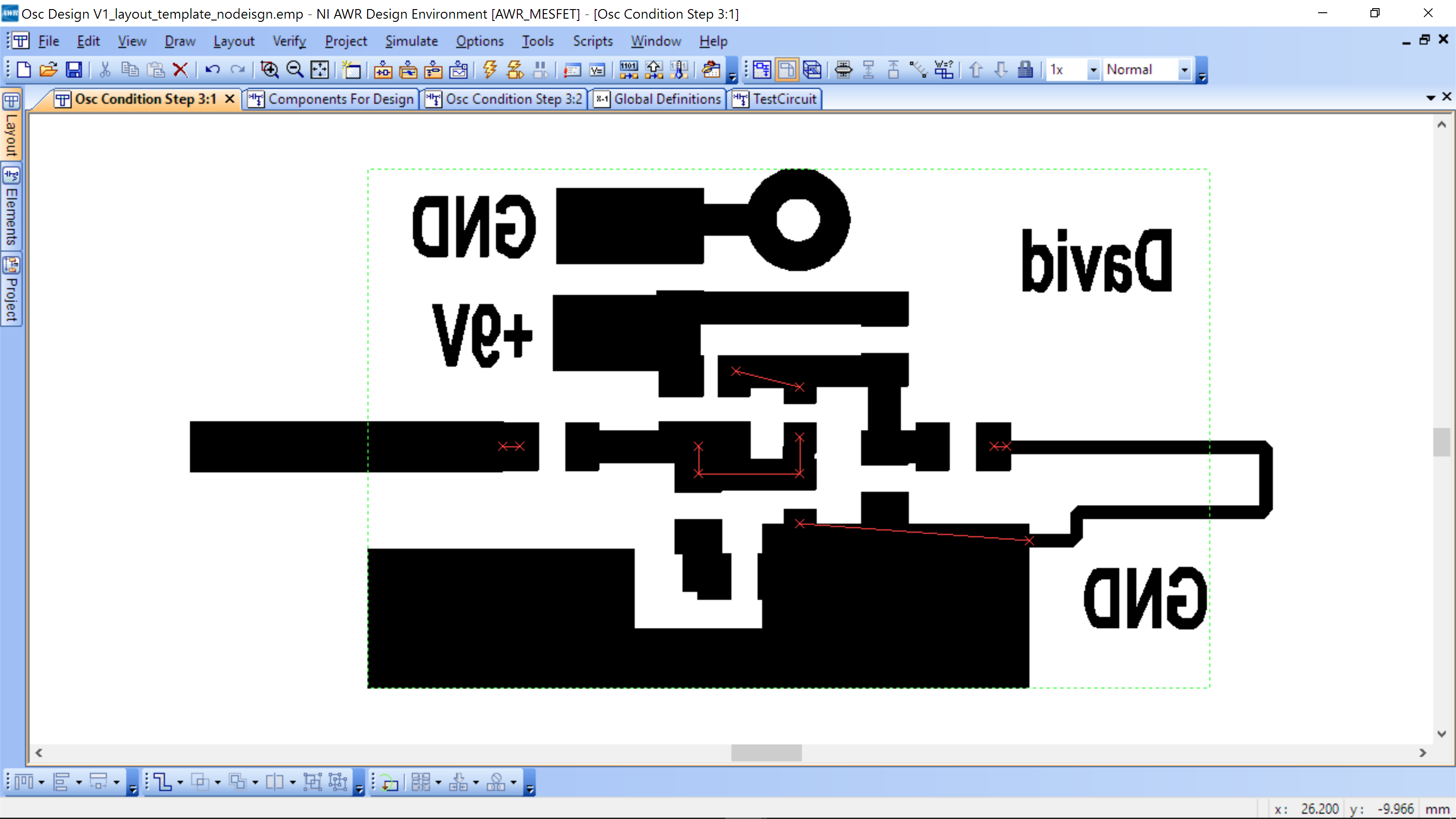
Your schematic for layout should look like the following (same as for the OSCAPROBE simulation), except now with your MLIN structure 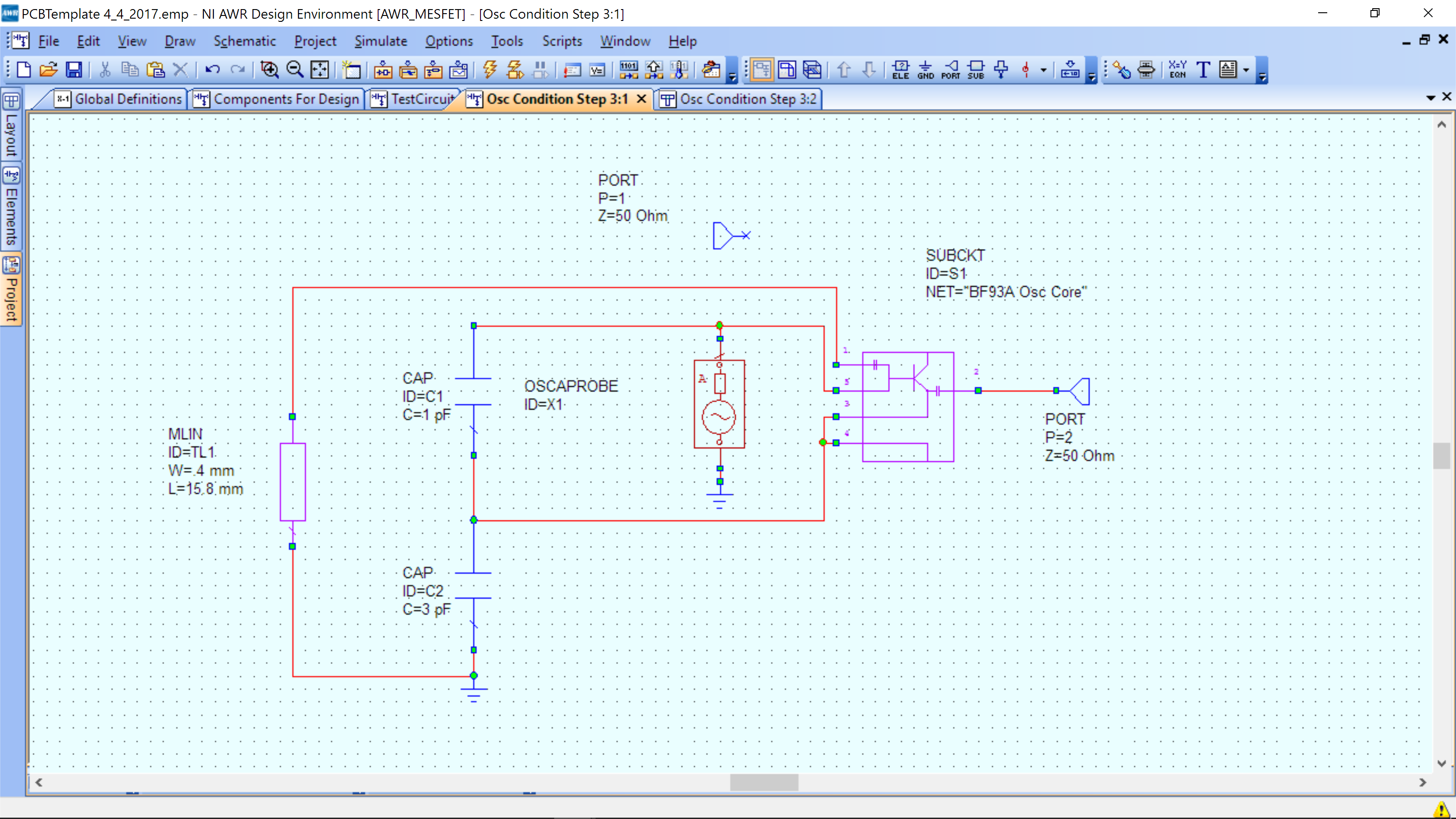
Click View->Layout and a layout will appear

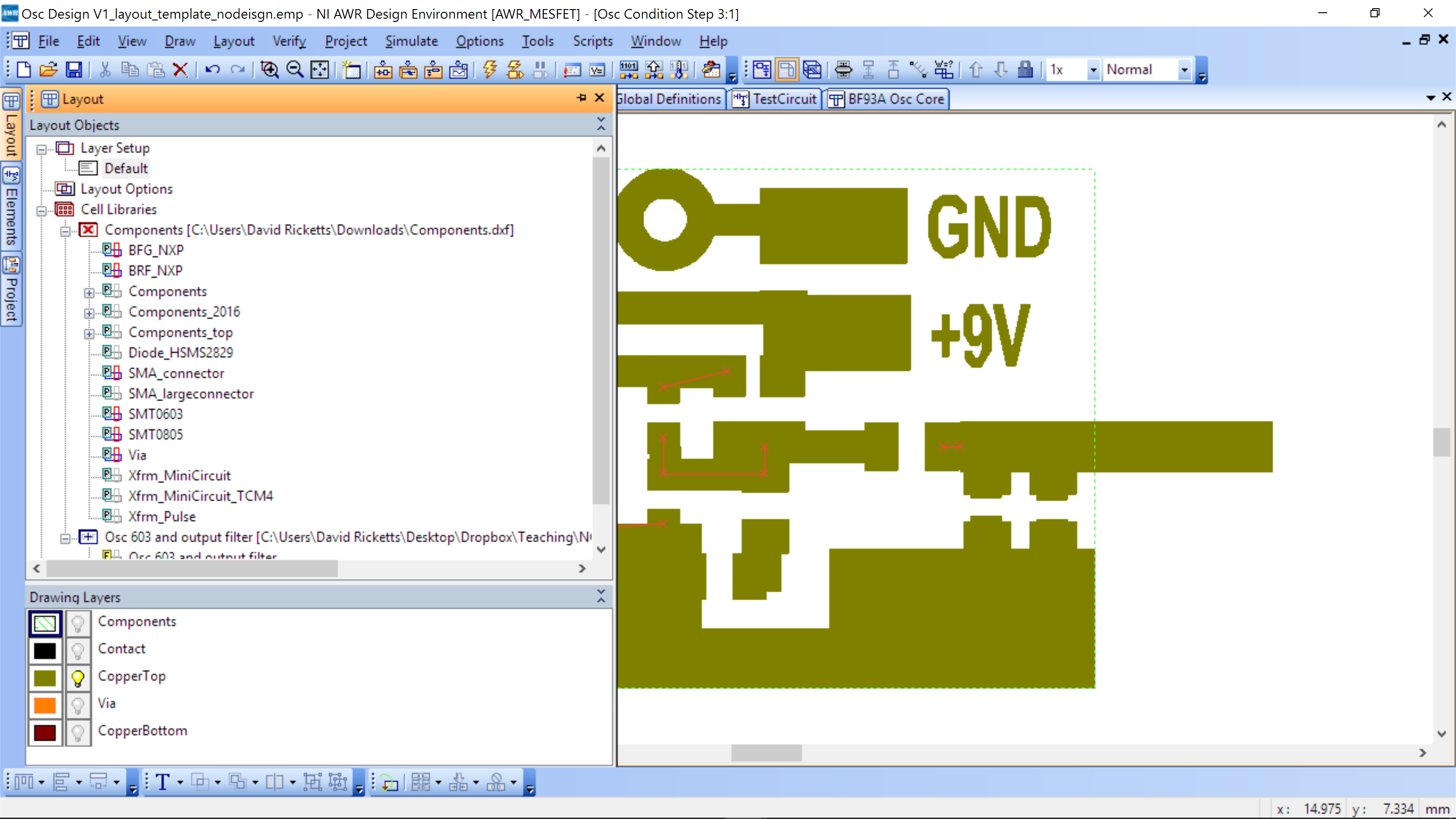
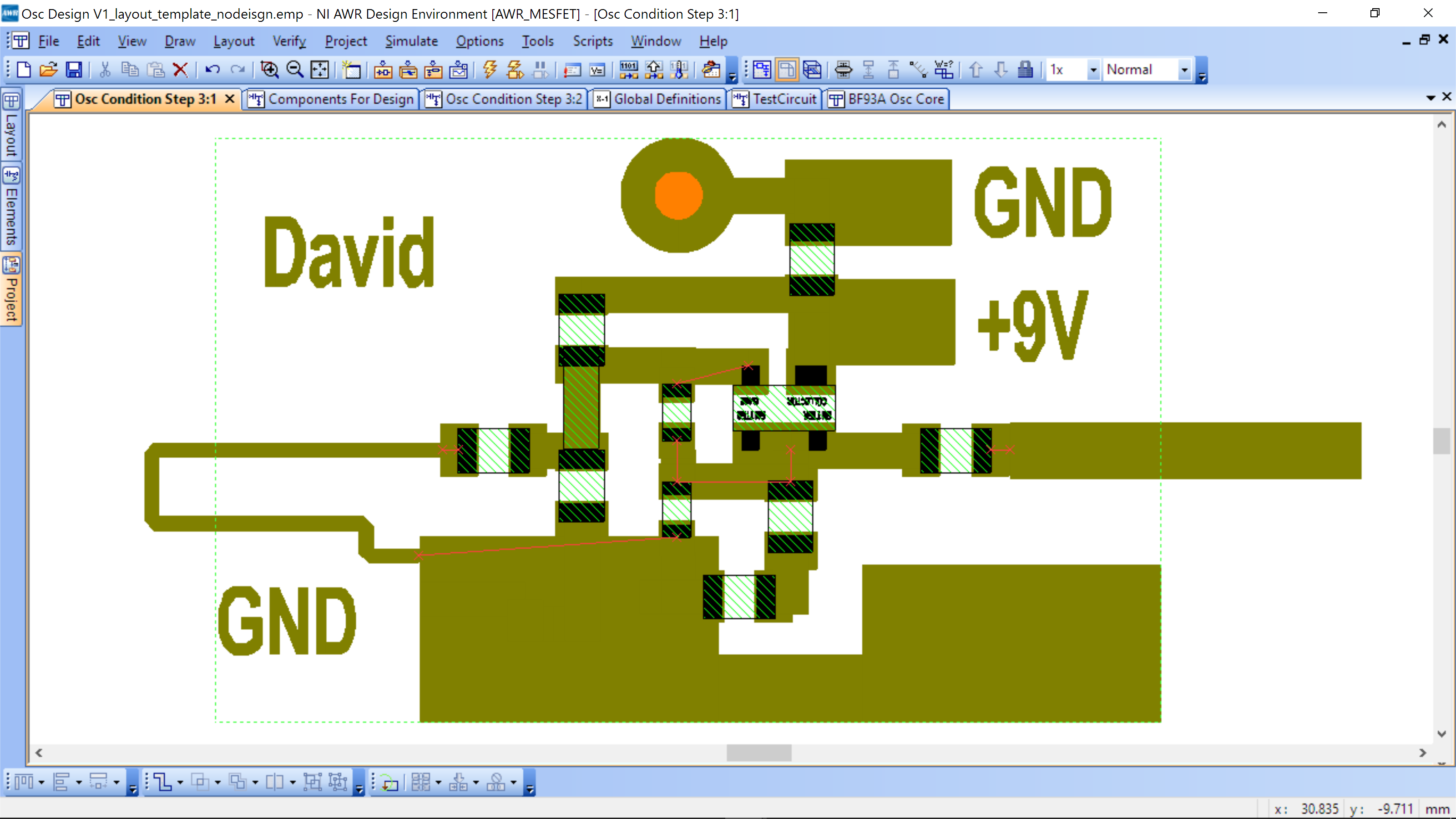
The transistor core has been laid out for you. You need simply add the feedback capacitors and then route the MLIN inductor. To add capacitors, return to the schematic, select each capacitor, then Properties->Layout->Library->Component->603 package. Two 603 packages will appear on your layout. Using the Edit menu to flip and rotate, you can orient them so that the they can be placed in their position below.
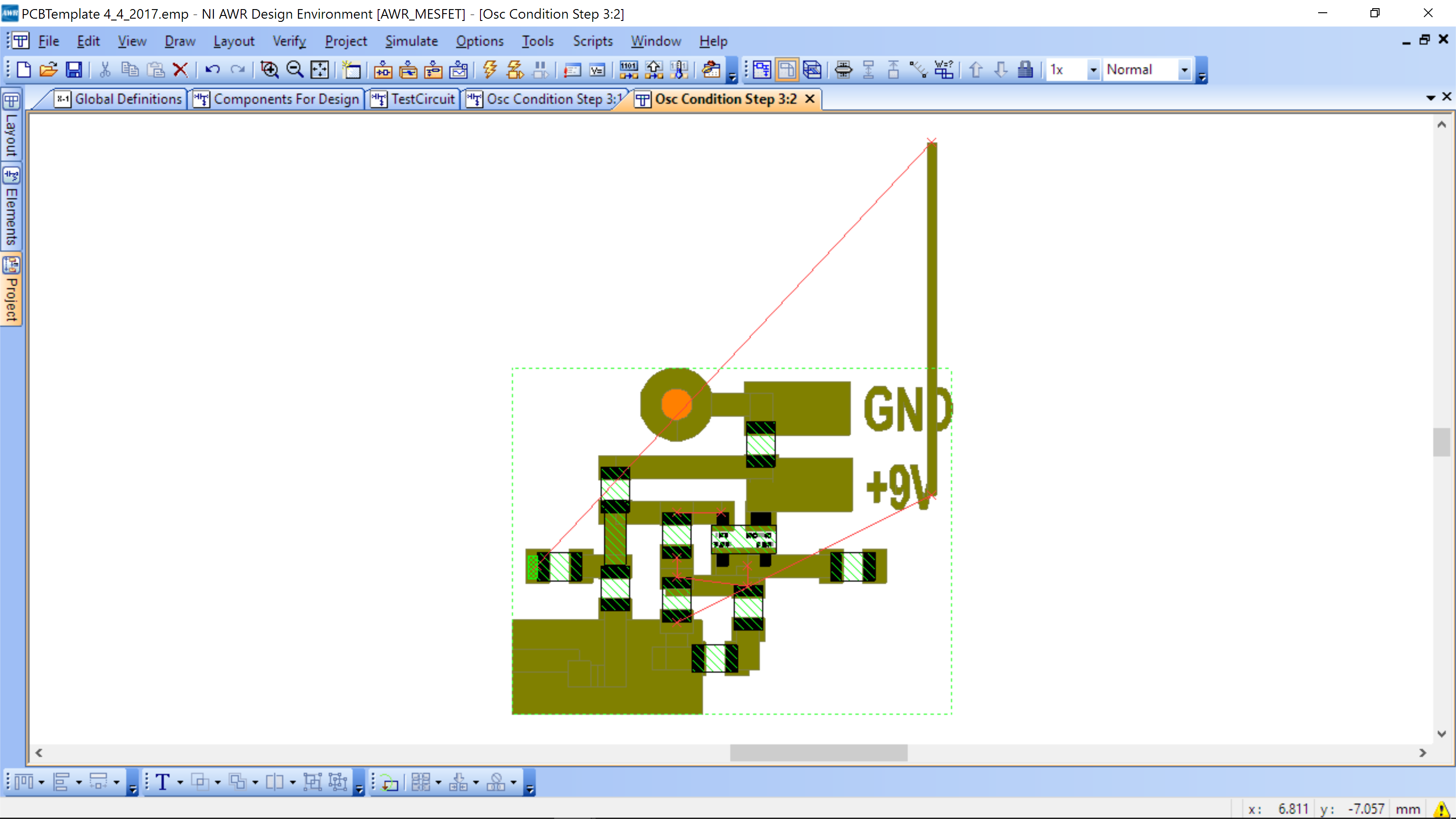
You can ignore the red lines in the oscillator core (bounded by the light green box) – they are for layout versus schematic check (LVS). The red lines to MLIN are showing the connectivity for that component.
The MLIN inductor is a straight piece of copper. We need to modify it to 1) connect to the input and GND on the left and 2) bend it to allow tuning. Replace the MLIN model by MTRACE2. You can do this by just changing the name of the component in Schematic view by double clicking MLIN name. Generate the layout with MTRACE2. You will notice that the layout view is not changed!
NOTE: In the following, make your MTRACE2 about 30% longer than your designed MLIN to allow for tuning.
Initially it appears the layout did not change, but the component is different.. Hover you mouse over one of the lines in the Layout view, you will see an arrow on one end (see figure (a) below). Now double click on the line, three handles apear at the beginning, middle and end of the line. Double click again on the handle which is at the end where the arrow was and you will notice that your cursor changes to a drawing path (see figure (b) below). You can now draw a path, for example to meander the line (see figure (c) below). Once you are happy with the shape you want the line to look like double click and the line will be re-drawn accroding to your path. (see figure (d) below).
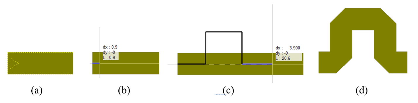
As you meander the length of the line will be noted. You must meander the line until it is the length you want – the layout will allow you go longer or shorter, so it is up to you to make it the correct length. When you are done routing, double click and the final shape will appear, e.g. (d) above. Now when you click the layout and the blue dots (handles) appear, you can move them to change the shape, but the length will be kept constant
.
Also note that even though you changed the shape of the line in Layout the symbol in the Schematic is still one straight line.
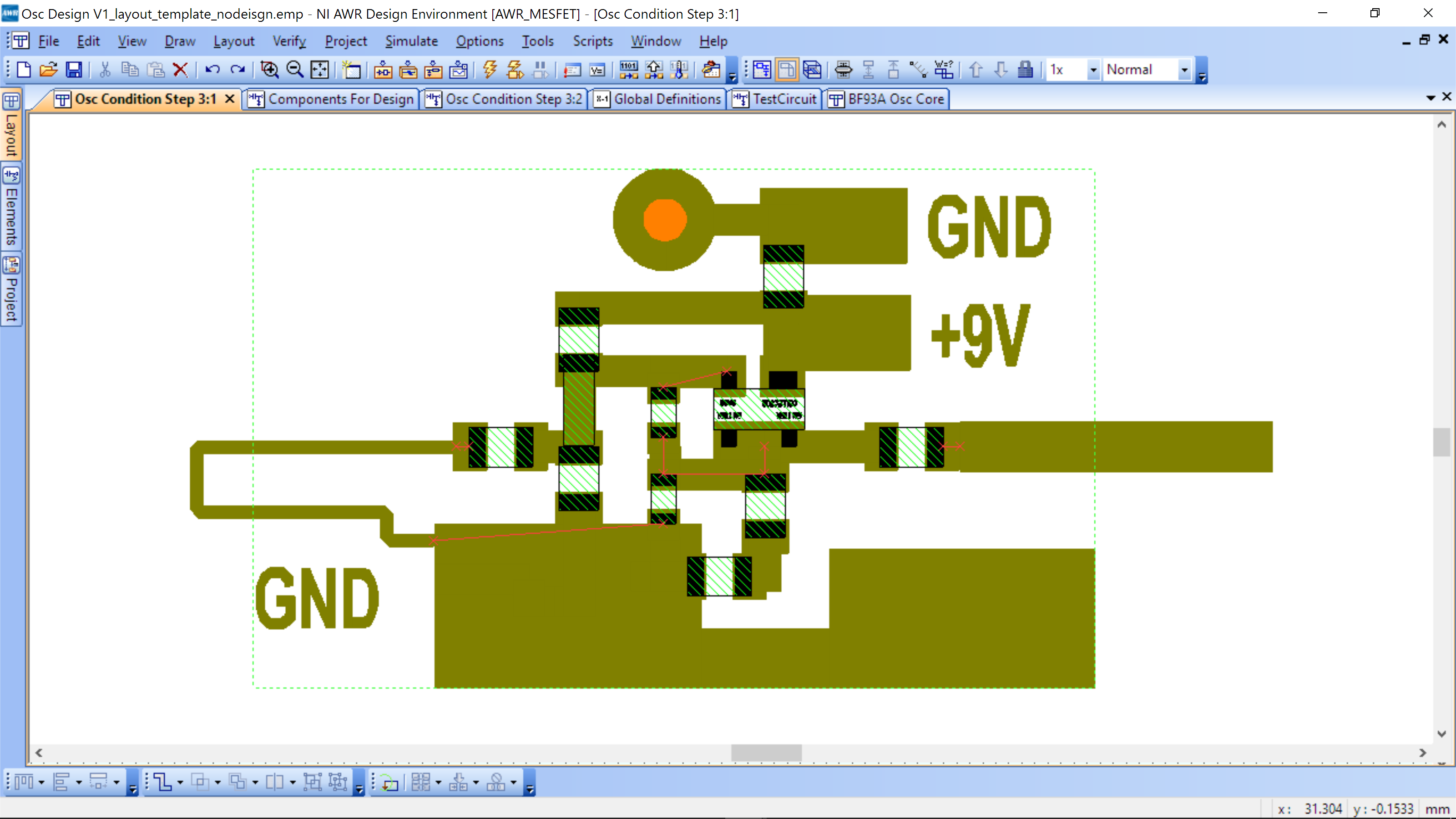
An example final layout is shown below.
The inductor to the left is laid out such that a short can be placed along the two parallel horizontal traces to make the inductor shorter. Build the oscillator as it is, then you can try tuning by placing a short piece of wire across the two parallel conductors.
Remember that you made the MTRACE2 longer than your designed MLIN for tuning. If not, return to layout and make it 30% longer.
Now add a MLIN of 50 Ohms (2.6mm wide) and at least 10 mm long to the oscillator output to extend the output away from the circuit. You will solder the SMA connector directly to this 50 Ohm line. The schematic looks like the following.
And the layout looks like this:
Fabrication
To prepare your design for fabrication, please follow the following steps:
- Add your name or initials to the design. Make sure they are away from the circuit, but do not increase the area of the design (find an empty spot to put them in).
- Right mouse click on the letters and Shape Properties -> Layout->Draw Layers select Copper Top. This will add it to the copper layer.
Go to the Layout tab on the left. On the bottom are radio buttons to turn on/off visibility of layers. Turn off everything, except top copper.
Go to the Layout tab again, under Layout Setup->Default, the following window will appear
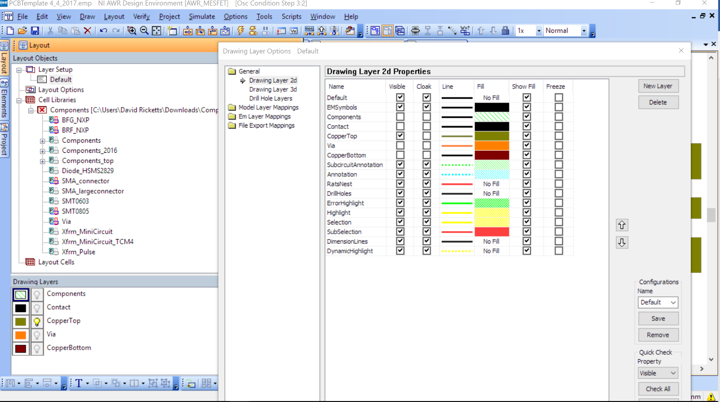
You will need to double click the Line and Fill for CopperTop and change the color to black. This is so when we print the layout, we get the darkest toner/color for our etching mask. Note the top of the pop-up box is for the line type or pattern, the bottom is the color. In the below “Solid” is selected as the pattern and the color “Black” at the bottom is selected.
The layout now looks like this
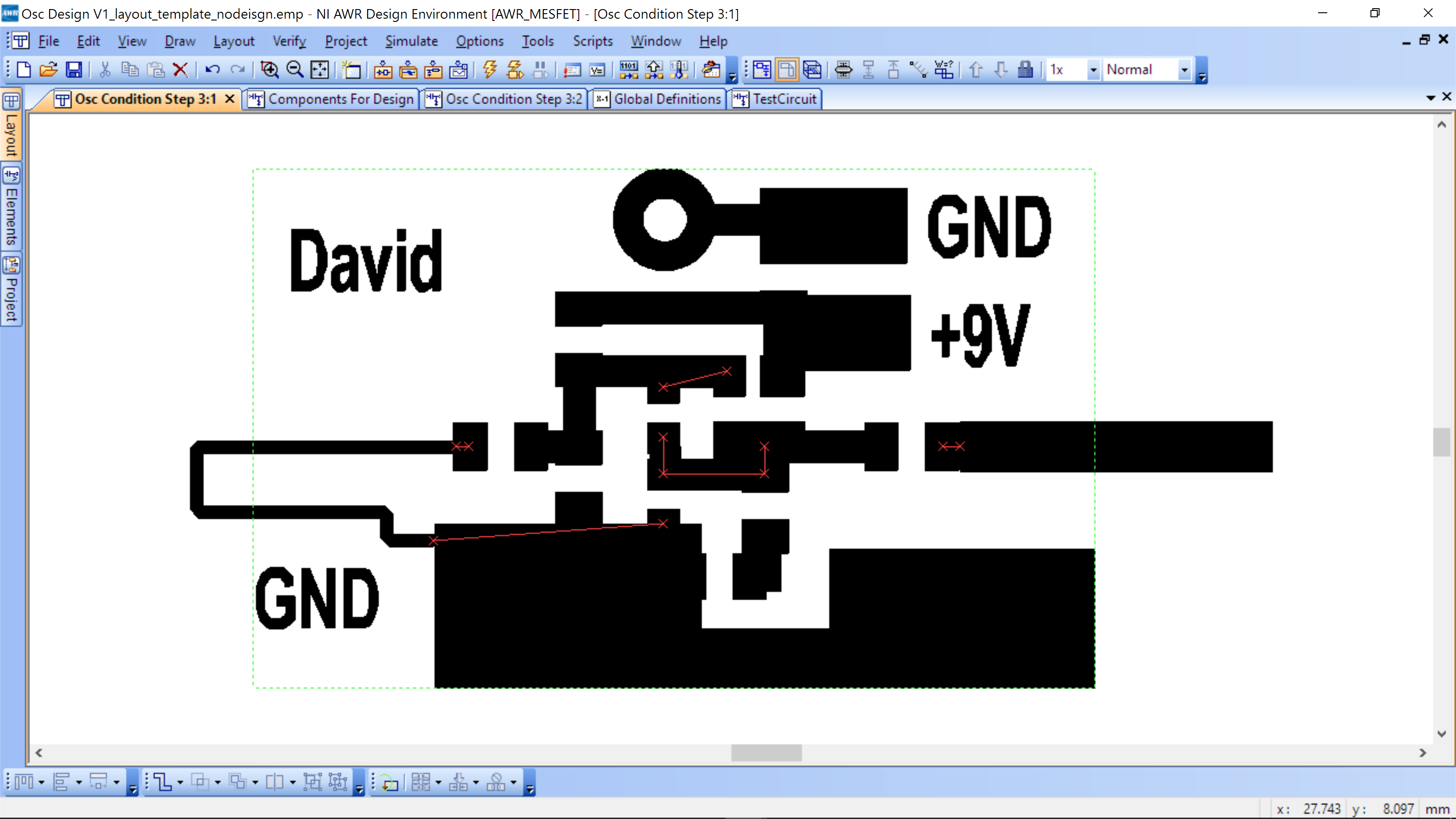
Now hit Ctrl+A to select all, then Ctrl-F (Also found in Edit menu) to flip. The cursor will change to ask you around which axis to flip. Left mouse click then move mouse up and you will see the layout flip around the vertical axis. It should look like this.
You will know its correct if the words are backwards!
Now export the file, Layout->Export-> set save as type as (DXF, Flat,*.dxf)
.
Go to the section/booklet on Fabrication
Assembly
The layout with components values is shown below. You can find the components from the color-coded sheet in your kit. Note there is a unique identified for each component, which includes a combination of: Number of components in kit, package style, number of pins, shape of pins, and finally color on packaging.
2.7k Ω
3pF
220Ω
1.5k Ω
200pF
1pF
Solder 9V Battery
Leads to pads
Use a small wire to short
Inductor for tuning
Solder SMA
To t-line
100nH
200pF
.1uF
BFG520
Test
Ensuring the 20 dB attenuator is on the Rx IN of the VNA, set the VNA to spectrum analyzer mode and set the frequency sweep to 650-1200 MHz. Your oscillator will likely be near 700 MHz when you first turn it on.
Place a wire on the left inductor and move it until your frequency is 950 MHz. It will be surprisingly easy to tune. Solder wire in place and check frequency. You can always re-adjust the frequency by moving the wire.
The output of the oscillator is 12-13 dBm, however the power of the pocked VNA is not calibrated, so you will only see the signal frequency.
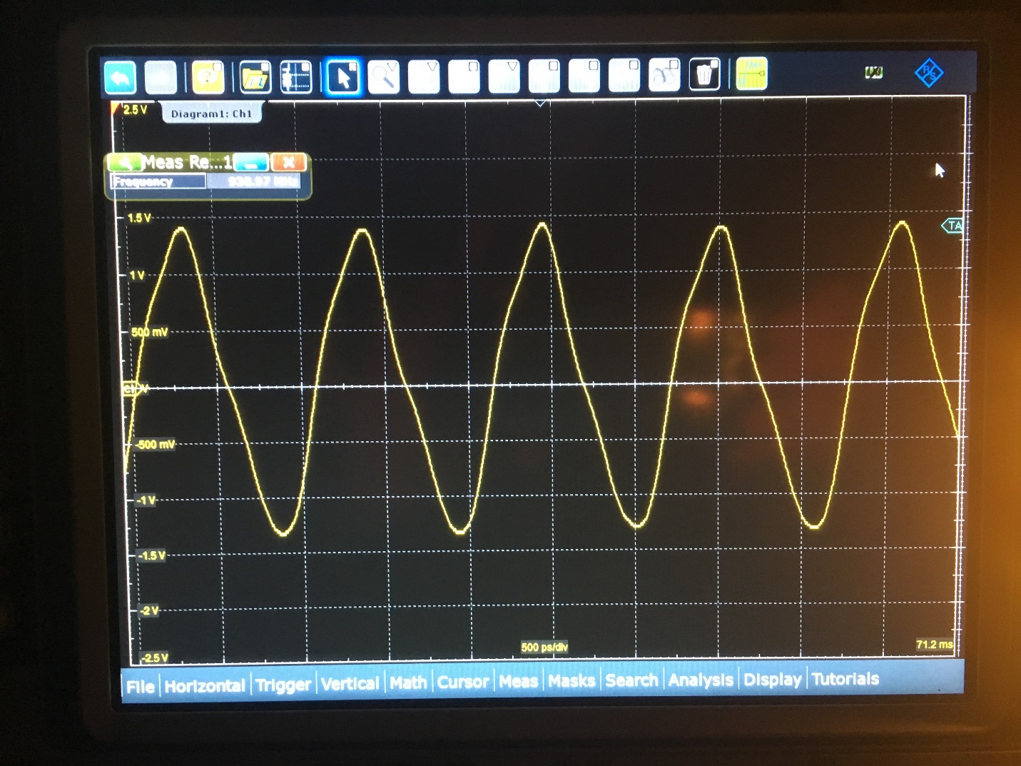
Below is a picture of the output from an oscilloscope (not measured as part of the workshop).