
Part 1 – Microstrip Line
Transmission line simulation
Create a new schematic in NI/AWR Design Environment and call it “t-line ideal”. Press Ctrl-L, type “TLIN” in the window which opens, and click OK button. An ideal transmission line is added to the schematic. Use the same procedure to add two “PORT”. Connect the three elements as shown in the figure below.
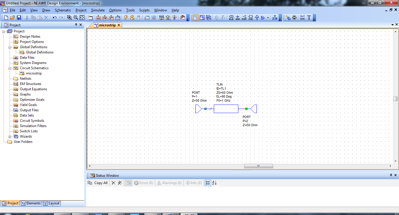
TLIN – A t-line model is defined by Z0, EL and F0. Z0 represents the characteristic impedance of the t-line. EL represents the electrical length of the t-line at frequency F0. , 360 degrees equals to one wavelength. . In your schematic set Z0=50Ohm, EL=90 deg, and F0=1GHz.
PORT – A port model is defined with Z. Z represents the port impedance looking into the port. Set Z=50Ohm for both ports in your schematic.
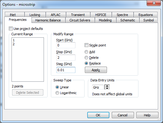
The frequency range over which you want to perform the simulation can be set for each schematic design or set by defualt for all schematic designs in the project. Here, you will set the frequency range of the “t-line ideal” schematic by right-clicking on its name under the project browser. Click Options from the menu and choose the Frequency tab. Unselect the “Use project defaults” box then modify the frequency range from 0GHz to 2GHz with step 0.01GHz. Make sure the “Replace” option is selected then click Apply. Frequencies will be shown on the Current Range box. Click OK button.
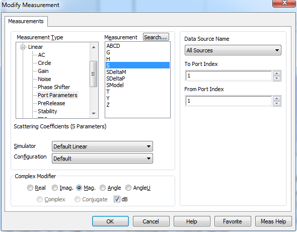
Right click on the Graphs node in the Project Brower. Click New Graph from the menu. Call this graph “T-line Sparams” and Select Rectangular for its type, and click Create. Once the graph is created right-click on its name and select Add New Measurement from the menu. In the Modify Measurement window, select Port Parameters on the Measurement Type and then select S on the Measurement.
Check Mag. and dB box at the bottom of window. On the right, choose 1 in the From Port Index and To Port Index box. This will plot dB(Mag(S11))
Click OK.
Add another rectangular graph and call it “T-line Phase”. Add a measurement to this graph and this time choose to plot Angle of S21 (From Port Index=1, To Port Index=2)
Nothing will be shown in the graphs until you hit the Simulate button on the top ribbon of the main NI/AWR Design Environment window.

Assignment (1 pts):
- For this ideal transmission line with Z0=50Ohm what should the value of S11 be with a 50 Ohm port? Does your answer match the simulation results?
- How much should Angle of S21 be at 1GHz?
Real microstrip line model simulation
When implemented as a real transmission line, characteristic impedance and electrical length should be specified by the physical dimensions of the line.
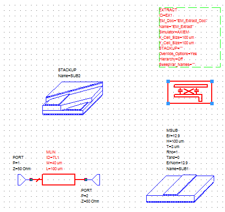
Create a new schematic and call it “t-line real”. Use Ctrl-L and add an “MLIN” microstrip line component. Also add two ports as before. In addition, add the substrate model “MSUB” into the schematic.
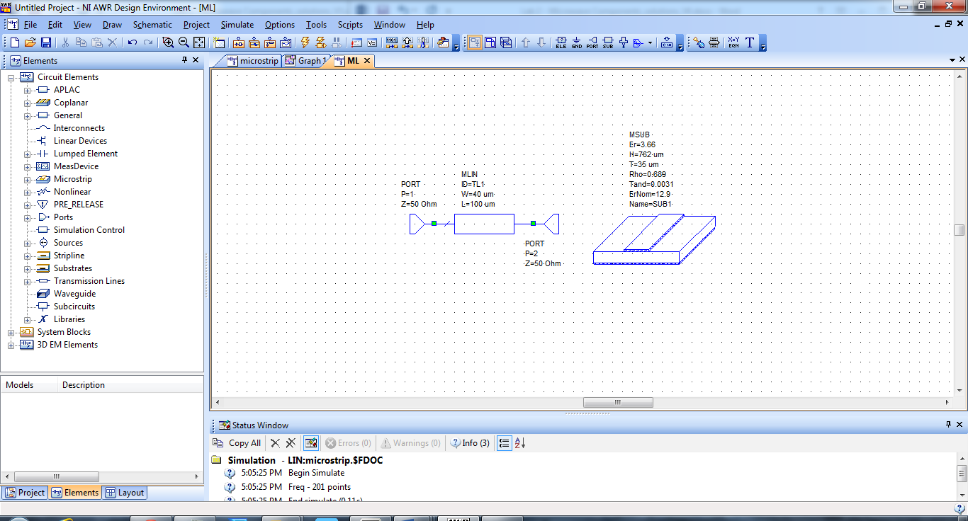
MLIN is a physical microstrip line with W and L. W represents the width and L represents the length. Note that the physical length is not the electrical length. The electrical length is a function of the physical length and the wave velocity.
W and L can be determined to provide a given Z0 and E using TXLINE tool in NI/AWR Design Environment, which will be introduced later.
MSUB is the Microstip Substrate model which is used to define properties of a substrate of the microstrip line. The five main parameters are Er, H, T, Rho, and Tand. Er represents the relative permittivity of the substrate. H represents the height of the substrate, T represents the thickness of microstrip line trace, and Tand represents the loss tangent of the substrate. Rho represents metal resistivity normalized to gold. Here, copper is used as the metal conductor. Set Er=3.66, H=762um, T=35um, Tand=0.0031, Rho=0.689.
TXLINE is a useful tool to calculate physical dimentions of microstrip line given the electrical characteristics and is launched from NI/AWR Design Environment main window, under Tools menu Tools>TXLine.
Choose the Microstrip tab.
Enter the Material Parameters on the top of the window. Also Heighy and Thickness under Physical Characteristic. These should match the values you entered in the MSUB component in the schematic diagram; Dielectric Constant=3.66, Loss Tangent=0.0031, Conductivity=5.96E+07S/m, Height=762um, Thickness=35um.
Enter the electrical characteristics of t-line on the left. Enter the same values you used in the previous part of the lab: Impedance=50Ohm, Frequency=1GHz, and Electrical Length=90deg.
Now you can click the right arrow button near the center of the window to synthesize the transmission line. The result shown in the Physical Characteristic is the physical length and width you should use for MLIN model.
Assignment (2 pts):
- Set the frequency range of the new schematic to 0GHz to 2GHz with step 0.01GHz and run the simulation again. Compare the magnitude of S11 and Angle of S21 of the two tline models.
- Right Click the schematic design “t-line real” and select View layout. The layout of the single microstrip will be shown automatically. Insert the screenshot of the layout of the microstrip line. Can you do the same for “t-line ideal”? why?
Microstrip line EM simulation
Even though MLIN models the actual microstrip line on a substrate it does not take into account all the physical behaviours of the line, most importantly the electromagnetic coupling between adjacent lines. These effects can be studied by Electromanetic (EM) simulation. The drawback of EM simulation is the longer time and computataional resources it requires. In many real projects, the initial design is optimized with MLIN model and finally only verified by EM simulations.
In order to perform an EM simulation on your transmission line, open the schematic diagram “t-line real”. Then from the Scripts menu, select EM and then creat stackup.
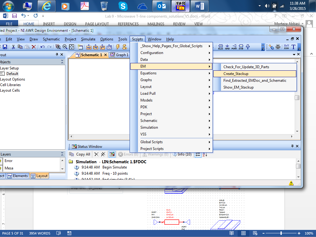
In the window which opens, set the grid to 100um and then press OK. This will add two new components to your schematic design, STACKUP and EXTRACT. These will produce the required files for the EM simulations.
Note that not all the component in your design will be included in EM simulation. You need to explicitly select the transmission line (or multiple of transmission lines, if there are more than one) which you want to have EM simulated.
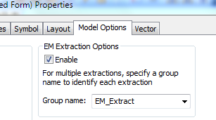
Select the MLIN component, right-click and select Properties. On the Model Options tab, select the Enable under the EM Extraction Options.
Now when you select the EXTRACT component in the schematic window, the transmission line(s) which will be included in the EM simulation will be highlighted.
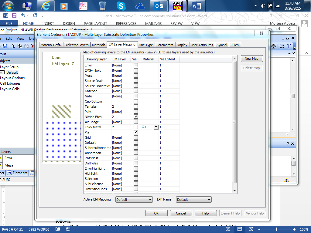
One final step is needed before you start the simulations. Double click on the STACKUP component and under the tab EM Layer Mapping, select CU as the material for Thick Metal.
You can now run the simulation and see the performance of the EM simulated microstrip line, to the MLIN model and ideal TLIN.
Assignment (1 pts):
Compare and plot the simulated results from the three models of the microstrip line.
Can you explain why there is or there is not large differences between these results?
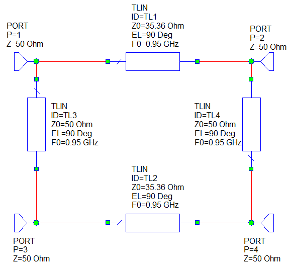
Part 2– 3dB Branchline Coupler
In this part of the lab you will design a 0.95GHz 3dB Branchline coupler circuit. The branchline coupler has the following parameters:
Zh: Characteristic impedance of the horizontal t-lines
Zv: Characteristic impedance of the vertical t-lines
EL: electrical length of transmission line
Z: impedance of the 4 ports
F0: operating frequency
Create a new schematic design and call it “BranchLine ideal”. Add four TLIN elements and four ports and connect them as shown below. Set Zh=35.36Ohm , Zv=50Ohm, EL=90deg, Z=50Ohm, F0=0.96GHz. How these values are derived is explained in the lecture noted.
Assignment (2 pts):
- Set simulation frequency range from 0 to 4GHz with steps of 0.01GHz. Plot the magnitude of S11 (port 1 to port 1), S21 (port 1 to port 2), S31 (port 1 to port 3), and S41 (port 1 to port 4) in dB scale in a Rectangular graph. Add marker on S11 and S31 curves at 0.95GHz.
- Which ports are isolated and by how much?
- Which ports are coupled – what, if any, is the insertion loss?
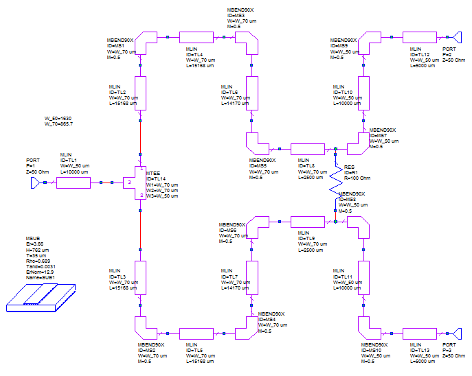
Create a new schematic and call it “BranchLine real”. Add four MLIN elements, four ports and an MSUB. Set substrate definition Er=3.66, H=762um, T=35um, Rho=0.689, tanD=0.0031 in MSUB.
Determine the Width and Length of the transmission lines using TXLINE and bulid the real Brachline coupler schematic.
Assignment (2 pts):
- Insert the screen shot of the schematic of the real Brachline coupler schematic. (1 pts)
- Set simulation frequency range from 0 to 4GHz with steps of 0.01GHz. Plot the magnitude of S11 (port 1 to port 1), S21 (port 1 to port 2), S31 (port 1 to port 3), and S41 (port 1 to port 4) in dB of the real Btanchline coupler model in Rectangular graph. Add marker on S11 and S31 curves at 0.95GHz. (1 pts)
- Compare to the ideal transmission line circuit – what has changed?
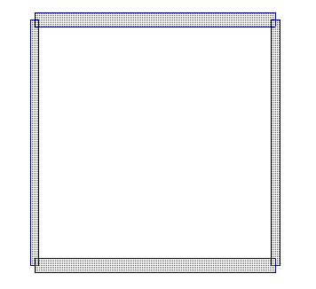
Right click on the “BranchLine real” under the Circuit Schemtics in project browser and select View Layout. The layout window will open and below is an example of how it may look like.
This means orientation of the 4 transmission lines with respect to each other is not known even though you placed them perpendicular in the schematic. The red dashed lines indicate where an electrical connection is made. You can select one of the lines and move it around with your mouse and you will see that the red lines still shows the correct electrical connection.
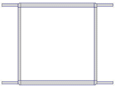
Try to re-arrange the lines, and rotate them to the correct orientation until all the red lines disappear. If you are confused which component in the layout correspond to which transmission line in the schematic, you can have both schematic and layout views side by side, and see that every time you select an element in one view, its corresponding element in the other view is highlighted. If you placed everything correctly your final layout should look like this.
As you see lines overlapp which each other in the corners resulting in the effective length of lines to be shorter than what you specified. Also there are discountinuities where lines meet, and there is no clear point where input and output connectors (represeted by ports in the schemtaic) should be attached on the PCB.
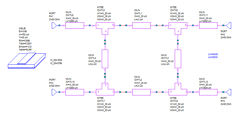
In order to fix these problems we will add a few new components to the schematic.
MTEE$ – A T-junction with three edges widths W1, W2, and W3. The width of W1, W2, and W3 is set automatically to the same width of tline which T-junction is connected to.
Also lets add short pieces of additional microstrip line MLIN between each port and T-junction. If you keep characteristic impedacne of these transmission lines to 50Ohm, they will just act as extention to the 50ohm ports and will not affect performance of the coupler. Schematic of the modified real Branchline coupler is shown below.
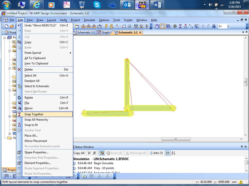
Try to view the layout of the Branchline coupler now. As shown in the figure below, lines are at correct orientations but still not properly arranged. Select all the components (Ctrl+A) and under edit menu select Snap Together. This will re-arrange the lines to form the final layout of your coupler.
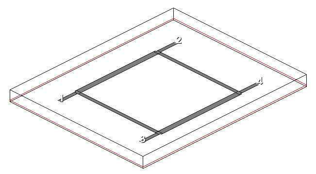
You can also see the 3D view of the layout.
Note that generating and correcting the layout does not affect the simulation results of the coupler, since NI/AWR Design Environment uses the symbols in the schematic view and the layout view. It is however important to have the correct layout of the coupler for EM simulations.
Assignment (2 pts):
Do the procedure explained in the previous section for t-line to creat a stackup and compare the EM simulation results with the TLIN and MLIN models. Explain the differences
Part 3– 3dB Wilkinson Power Divider
In this part of the lab, you will design a 0.95GHz 3dB Wilkinson Power Divider circuit.
Wilkinson Divider has the following parameters:
Z: port impedance
Z0: characteristic impedance of the transmission lines
EL: electrical length of the transmission lines
R: isolation resistance
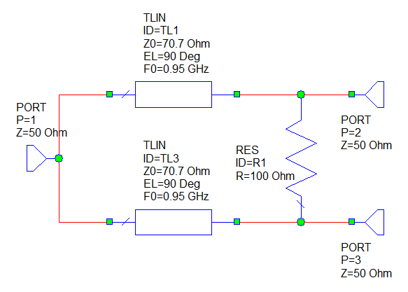
Creat a schematic and call it “Wilkinson ideal”. Add two TLIN elements, one RES and 3 ports. Connect them as shown below and set Z=50Ohm, Z0=70.7Ohm, EL=90deg, R=100Ohm.
Assignment (1 pts):
- Set simulation frequency range from 0 to 4GHz with steps of 0.01GHz. Plot the magnitude of S11, S21 , and S31 in dB in Rectangular graph. Add marker on S11 and S31 curves at 0.95GHz.
Create a new schematic and call it “Wilkinson real” and make the same wilkinson divider with MLIN models. Do not forget to add MSUB and set its parameters as the previous sections of the lab. Use MTEE$ components at port 1. Also use MBENDA$ to implement bends in lines to save area on the layout. Your schematic could for example look like this. Note that sum of the 4 transmission lines between port1 and the point where RES is connected should be equal to the electrical length of your design.
Assignment (1 pts):
- Show the Layout View of the microstrip 3dB wilkinson power divider.
- Simulate magnitude of S11 and S21 and S31 in dB from 0 to 4GHz with steps of 0.01GHz. Compare to the real transmission line model.
Part 4 – Low Passband Filter (LPF)
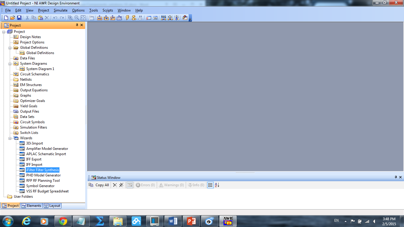
In this final part of the lab, you will design a low pass filter using the iFilter tool which is built in NI/AWR Design Environment. Open Wizards node in the Project Brower and double click on iFilter Filter Synthesis.
ifilter wizard is a very good tool to design filters of different type (Low Pass, Band Pass or High Pass) and in different implementations (lumped elements, transmission line, coupled lines, combline, etc). The tool also generated layout of the filter, which can be used to perform EM simulations.
On the main window of the wizard, under the Type- Approximation click on the button which says Lumped Elements.
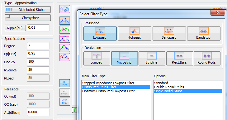
Change the settings accroding to the figure below to Lowpass microstrip filter with distributed single stubs.
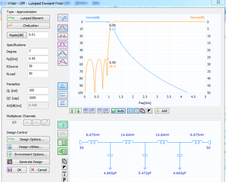
A filter’s performance is specified by different parameters like passband frequency (Fp), allowed passband ripple (in dB) and filter degree (order of the filter). Degree or Order of the filter determines how sharp the transition band between passband and rejection band is. There are often times requirements from the system on how much should a freqeuncy compoenent outside of the passband be attenuated (Remember the image rejection filter?). It is also important to specify to specify values of the source and load impedances. These are usually set to 50Ohm unless stated otherwise.
For your design set Ripple=0.01, Degree=7, FP=950MHz, Rsource=50, and Rload=50.
Note how performance of the filter which is shown in the wizard changes as you increase the degree, or Ripple.
For Microstrip filter implementation two additional parameters are needed.
Zo: impedance of the microtrip line of LPF
Att: attenuation loss per length of the microtrip line
For this design set Zo=100, Att=0.008dB/cm.
You also need to set the substrate information and fabrication constraints. Click on “Design Options” button and then “Technology” tab and enter the substrate parameters:
Substrate Er=3.66, Height=762um, Cond.Thickness=35um, tanD=0.0031.
Then go to “limits” tab and set Min Width and Min Spacing of the printed structures to 75um.
This tells the software than lines narrower that 75um or closer than 75um are not practically feasible so optimize the design to avoid dimension smaller than these.
You can now switch between the schematic view and layout view of the filter in the wizard.

Add markers with the  and quickly check microstrip LPF ideal performance.
Once you have entered all the settings, and you are satisfied with the performance and look of your filter you can generate an NI/AWR Design Environment schematic design from the tool. Click on the “Generate Design” button in the left down bar. Save Base Name as “LPF” and click “OK”. Exit the wizard by clicking on OK button.
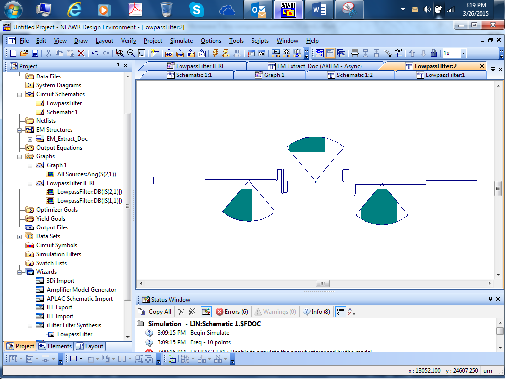
Open the schematic view of the filter. Here you can see that NI/AWR Design Environment has used standart elements to implemet the filter. There are some new elements like the MSRSTUB2 and MTRACE2 which you may not have seen before. These are radial stubs and meandered lines. You should be able to recognize these components from the generated layout views.
As your design gets more complex and you use elements other than straight microstrip lines, EM simulation becomes more important. For example, closely spaced staructures may have electromagnetic couplings which are NOT included in the schematic and can only be seen after EM simulations. Some of the critical parts are marked in the figrue below.
Assignment (3 pts):
- Set up the EM simulation of the filter the same way you did earlier for the t-line and compare the magnitude of S21 and S11 in dB to schematic design. Explain the reason for any differernce
Part 5– Band Passband Filter (BPF)
Assignment (5 pts):
- Design a passband microstrip edge coupled standard filter with Ripple=0.01, Degree=5, Fo=950MHz, Rsource/Rload=50, Att=0.008dB/cm on the same substrate as previous section. Include a screenshot of the schematic view and layout views.
- Present magnitude of S21 and S11 in dB for schematic and EM simulations. Explain the reason for any differernce
Comments are closed.