
Part 1– Single Diode
Open Mixer_LAB_start_components_v1 NI/AWR Design Environment file. Note that his is a Schematic and not a System Diagram as we will be simulating real components. The values of components are taken from the examples in RF Electronics Design and Simulation, by Cornelis Jan Kikkert BE, PhD. All simulations and results are from schematics assembled independently from the design files made public by Dr. Kikkert and NI/AWR Design Environment.
The components are disabled. You can enable them by right mouse-clicking and Toggle Enable.
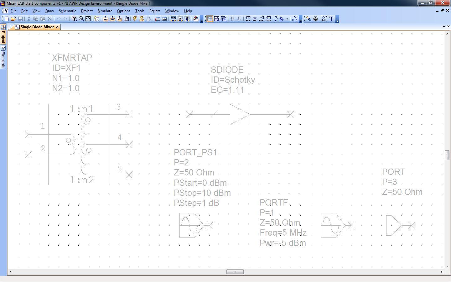
The blocks are:
- XFMRTAP – This is a simple transformer with turns ration n.
- SDIODE – This is a Schotky diode, a type of diode with a low turn-on voltage
- PORT_PS1 – This is a 50 ohm port, like a VNA, that will sweep the input power from PStart to PStop in PStep. In this lab we use 0 to 10 dBm in 1 dBm steps.
- The frequency of the input is not explicit but rather is implicit and is set by going to Options->Project Options and selecting the Frequencies tab. Select Single Point then type in 0.105 in the Point box and hit the Apply button. You will see it appear on the left box under Current Range.
- PORTF – This is a 50 ohm port, like a VNA, that has a specified frequency and input power. It is set for 5 MHz and -5 dBm.
- PORT – This is a 50 ohm port, like a VNA. It does not have any input power, but rather is used for measuring and 50 ohm termination.
We are going to start by setting up a simple diode with two ports. Assemble the following schematic from your start file.
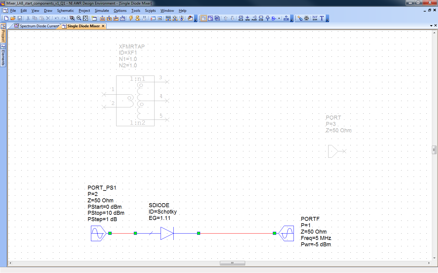
The simulation engine you will use is Harmonic Balance for time domain simulation, as described in previous labs.
Assignment (2):
- Plot the spectrum of current through the diode. To do this, add a Rectangular graph and then add a measurement. For these time-domain simulations, select Nonlinear->Power->Pharm. Select Port_1. The Sweep Freq should be set to 105 Mhz and Port_2 power should be set to 7 dBm. Select Mag and dBm. Click apply and it will plot the power spectrum of Port_1 versus frequency with port 2 having an input power of 7 dBm (remember Port_2 is a swept port, so this is telling it to plot only for Pin=7dBm). Scale your frequency axis so that the max is 300 MHz. (1 pt)
- What are the frequency components around 105 MHz (put markers on them to measure)? Are these what you would expect for a multiplier, i.e. the sum and difference of 105 Mhz and 5 Mhz? (1 pt)
We now need a way to extract the RF signals we want from the diode current. One way to do this is have a path for the IF current that is separate from the RF current. Since they are at very different frequencies (100 and 110 Mhz vs. 5 Mhz) a simple filter will do. Construct the following filter, also known as a diplexer.
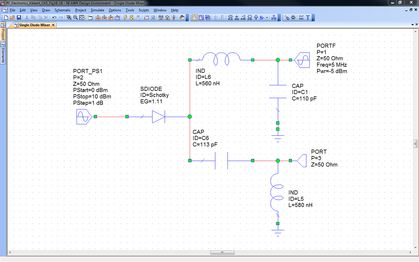
The low frequency component (including any DC bias) will pass through the inductor to the IF port. The RF frequencies will pass through the capacitor to the RF port. All currents will pass through the LO port.
Assignment (5 pts):
- Plot the spectrum of current at the RF port for the LO=7dBm (use same setting as in the previous setup). Put markers on the important frequencies. (1pt)
- Calculate the conversion gain and the LO-RF Isolation. (1pt)
- Now plot the conversion gain versus input power on the LO. Create a rectangular plot and then add Measurement Type->Nonlinear->Power and Measurement: LSSnm. This stands for “large signal S-parameter at harmonic.” This means the equivalent S-parameter at 105 Mhz. Set the To port to the RF port and the From to the IF port. Set the Harmonic Index to -1 and 1 for 100 Mhz and 0 and 1 for the 5 Mhz Harmonic Index. This tells the system which harmonic to measure. Set Sweep Frew to 105 Mhz and Port_2 to “use for x-axis”. This will set the x-axes to the swept power on Port_2. So this measurement will plot the S-parameter power from IF to RF (S21) for each LO power. (1pt)
- Plot the isolation between the IF to RF and LO to RF. Use the same technique as above, except add LSSnm lines for LO to RF port. Choose harmonics for both so that it is 105 Mhz (the LO freq). You can click the “…” bo next to the Harmonic Index to see how the Index corresponds to a frequency or you can just play with the up/down to make sure you get the correct frequency on both ports at 105 MHz. For the IF to RF, plot LSSnm but at the 5 Mhz harmonic (the IF frequency). (1pt)
- Does the conversion gain and LO to RF isolation match your calculated values from the spectrum plot? (1pt)
Part 2– Balanced Diode Mixer
Using your previous design, add another diode and transformer as shown below. This forms the balanced diode mixer discussed in lecture.
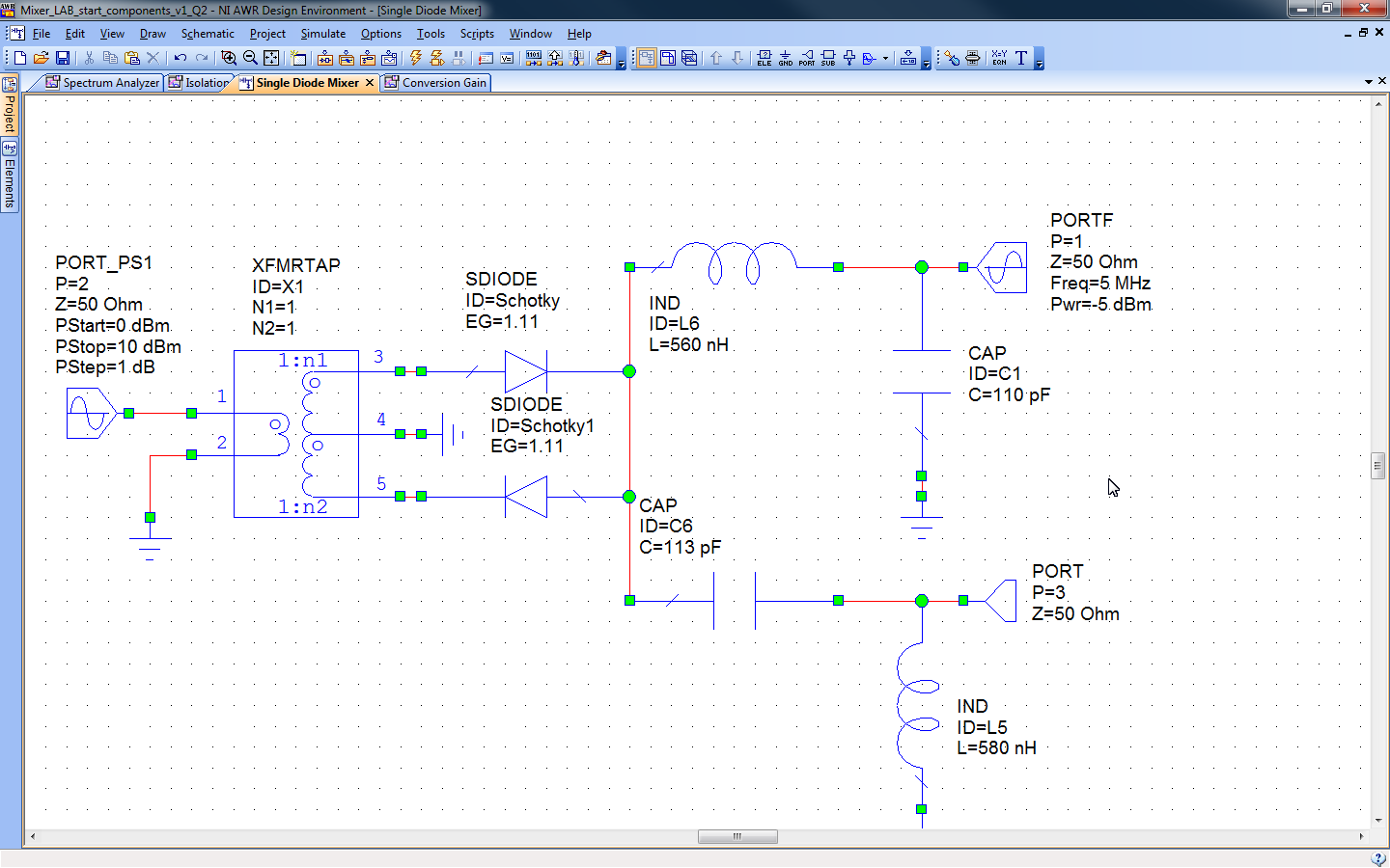
Assignment (5 pts):
- Plot the spectrum of current at the RF port for the LO=7dBm (use same setting as in the previous setup). Put markers on the important frequencies. (1pt)
- Calculate the conversion gain and the LO-RF Isolation. (1pt)
Conversion gain is -10.6 dBm –(-5 dBm)=-6.8 dB. Isolation: 7 dBm-(-58.5 dBm)=65.5 dB
- Now plot the spectrum of the current through one diode. This can be done by adding a MProbe to one side of a diode and then plotting the Nonliner->Current->Iharm in a rectangular plot. Comment on the differences/similarities with the harmonic plot for the RF port.
- Now plot the conversion gain versus input power on the LO. (1pt)
- Plot the isolation between the IF to RF and LO to RF (1pt)
- Does the conversion gain and LO to RF isolation match your calculated values from the spectrum plot? (1pt)
Part 3– Double Balanced Diode Mixer
Create a double balanced mixer using the diagram in the lecture
Assignment (5 pts):
- Plot the spectrum of current at the RF port for the LO=7dBm (use same setting as in the previous setup). Put markers on the important frequencies. (1pt)
- Calculate the conversion gain and the LO-RF Isolation. (1pt)
- Now plot the spectrum of the current through one diode. This can be done by adding a MProbe to one side of a diode and then plotting the Nonliner->Current->Iharm in a rectangular plot. Comment on the differences/similarities with the harmonic plot for the RF port.
- Now plot the conversion gain versus input power on the LO. (1pt)
- Plot the isolation between the IF to RF and LO to RF (1pt)
- Does the conversion gain and LO to RF isolation match your calculated values from the spectrum plot? (1pt)
Part 4– Microwave Mixer – For your project (not this lab)
C. J. Kikkert has created a complete NI/AWR Design Environment design of a microwave mixer including transmission line balun and filters. You can find his entire book and files at https://www.awrcorp.com/professors-in-partnership/professor-keith-kikkert/rf-electronics-design-and-simulation .
The NI/AWR Design Environment file: RF_Electronics_Kikkert_Ch5_Fig39-43 will be uploaded to Moodle and available directly per the license agreement for teaching use.
Comments are closed.