
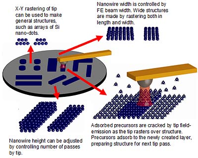
This uses tip-directed field emission chemical vapor deposition (CVD) for the precise fabrication of structures on the nanometer scale. Device geometry will be accurately determined by probe manipulation and controlled energy delivery at the probe tip. Significantly, this approach will enable control of length, width, orientation and height during fabrication. Tip-directed CVD will focus on the deposition of Si nanowires, using field-emitted electrons to locally crack adsorbed silane (SiH4) and disilane (Si2H6) through direct momentum transfer. In addition this research investigates methods for localized surface preparation, including the targeted desorption of hydrogen on a hydrogen-terminated Si substrate to localize the silane adsorption. This research I spart of the DARPA TBN program and is done in collaboration with Profs. Bain, Carley, Davis, Fedder, Sitti and Islam at CMU.
Comments are closed.