
Patch Antenna
Patch Antenna
In this part of the workshop you will design a 0.95GHz patch antenna. The theory of antenna operation can be seen in the following videos. The basics of operation is to generate a magnetic field out of phase with an electric field with a ratio that impedance matches with the air (377 Ohms).
At the bottom of this tutorial are three links to antenna basics and more detail on patch antenna theory.
In this part of the workshop you will design a microstrip patch antenna. The general dimensions are /2, however due to the specific dynamics of the antenna and the fringing fields, the exact dimensions require more careful calculations.
In antenna design, it is common to select a topology and then lookup the design equations for that antenna. Numerous reference books contain equations for antenna design for many types of antennas. We will first focus on the basic patch design and then examine impedance matching techniques.
The following video will provide design guidelines and a tutorial.
Transcription here.
For the microtstrip patch antenna, the following design procedure can be used:
- The width of the patch antenna (the part perpendicular to the feed line) is calculated as:
Where vo=3×10⁸, fo=950 MHz and er=4.5.The length of the patch (the portion parallel to the feed structure) is calculated in three parts.
- The effective permittivity is calculated as
![]()
Where h=1.53mm. (The height of the PCB).
- Due to the fringing fields, the electrical length of the patch is longer than its physical length. To compensate, a L is calculated.

- Finally the length can be calculated, accounting for the fringing fields, as:
![]()
Which is lambda/2-2 delta L.
You can use this online calculator to find the approximate values. Dielectric constant is 4.5 and thickness is 1.53 mm.
The input impedance can be calculated analytically, however we will find it using AWR/NI EM simulator.
To provide some intuition, the length of the patch is similar to a quarter wavelength transmission line. The width will affect the impedance. You will need to try adjustments in the simulation to get a feel for how to optimize your design for 950 MHz.
Building the basic patch
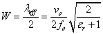
Load the example AWR/NI file on the workshop site (click here). This includes a small rectangular patch of copper. The file has loaded the default enclosure (surrounding space) and many of the fabrication properties.
Resize the patch to be the dimension you calculated above. To resize, you can double click the rectangle and you will see blue dots appear at the corners. You can simply grab and drag with the mouse. While dragging if you hit the space bar, a window will come up that allows you to type in the dx and dy of the new rectangle. Note that this is a delta and not an absolute size.
Once you have sized your patch, you need to add a port so the simulator can send in a stimulating wave. If you just added a port to one side of the patch, AWR/NI would stimulate the entire edge. To better approximate a real t-line port, draw a very small rectangle, 2.3mmx .1mm and place it at the center of the patch where the feedline would go. Below is an example.
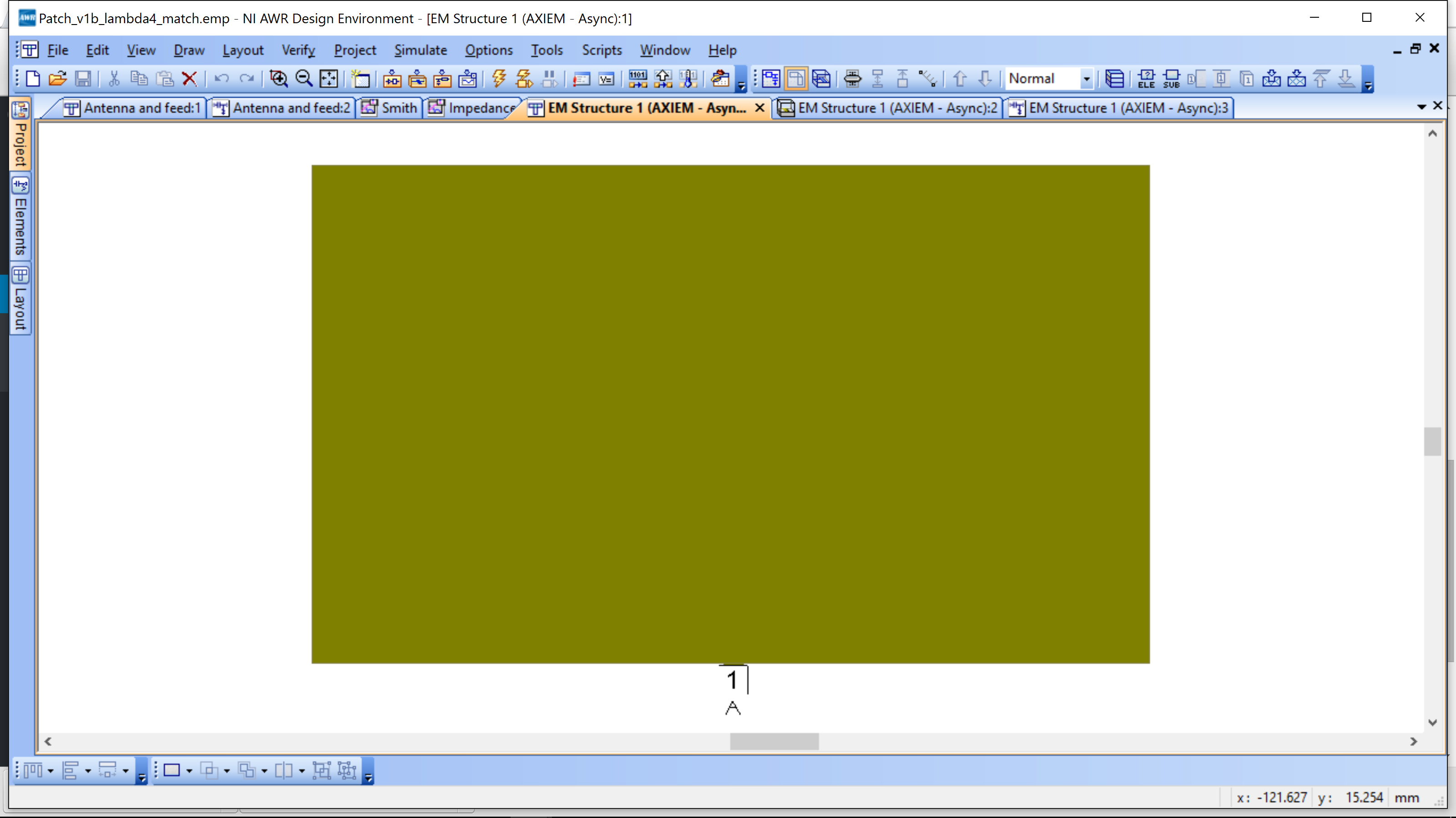
Below is a zoomed view of the small feed rectangle and the attached port.
The port can be added by selecting Edge Port (see below) and adding it to the lower edge of the small feed rectangle you created.
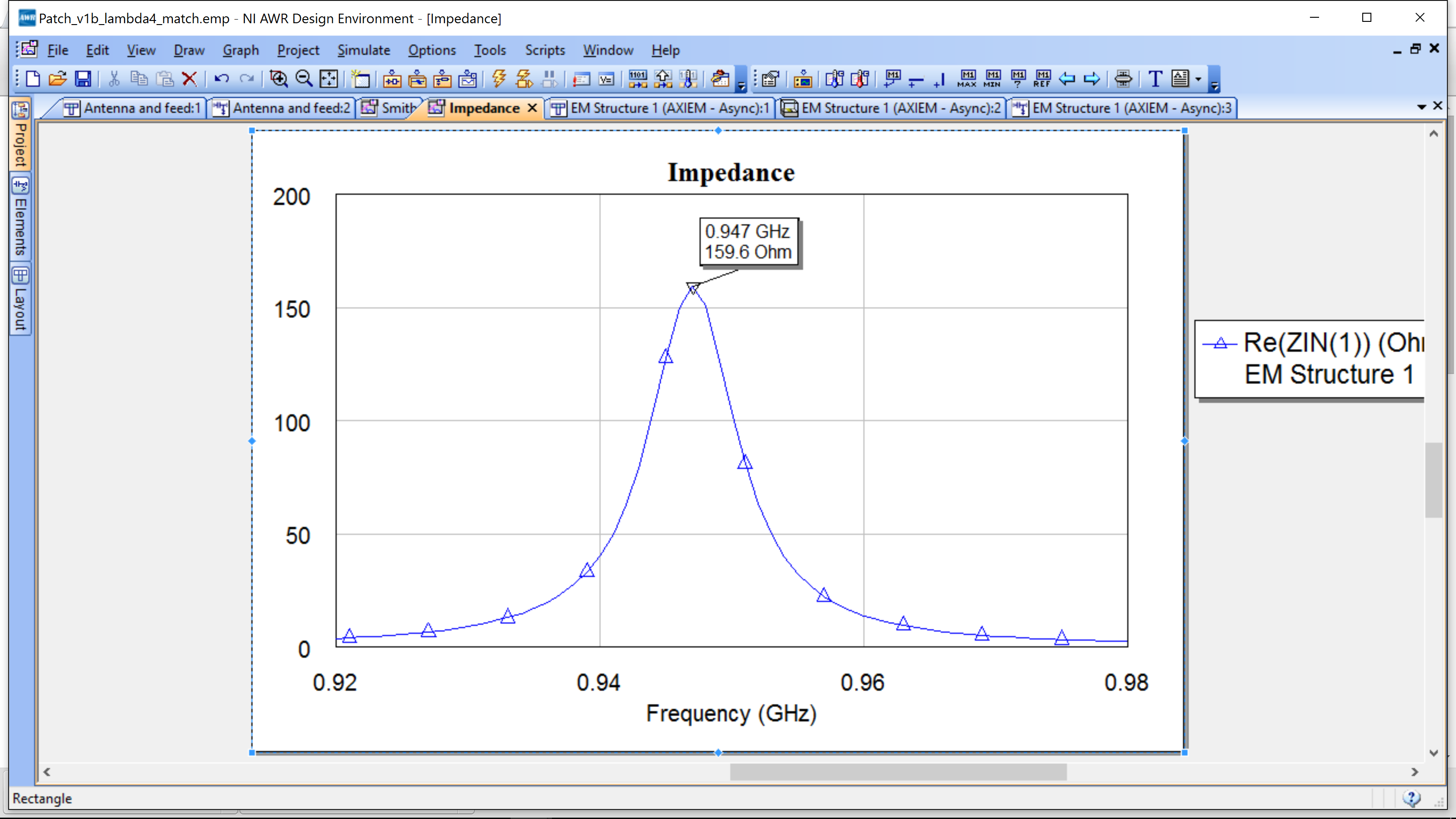
With the feedport added you can now run a simulation. To measure the resonance, Project-> Add Graph and then add measurement Linear->Zin. You will need to set the frequencies at which to simulate: Options->Project Options. Select a start and stop frequency to sweep over and the increment, then hit Apply. You may need to sweep a wide range if your shape is far off. Also, use 0.1 GHz as your increment, then refine until you can find a smooth curve, with a clear peak. At resonance (radiating frequency) the input should be real, and typically much higher than 50 Ohm – this is due to the patch structure, not antennas in general, however the real input impedance at resonance is a general property.
The impedance should look similar to the plot below.
Impedance matching I – /4 T-line
One of the simplest methods for impedance matching is to use a /4 t-line impedance transformer. You can find the length of a /4 line using the TXLINE.
TXLINE can be found under Tools-TXLINE. It is a calculator to help you convert electrical parameters such as electrical length and impedance to a physical implementation. The following screen shot show the calculator interface.
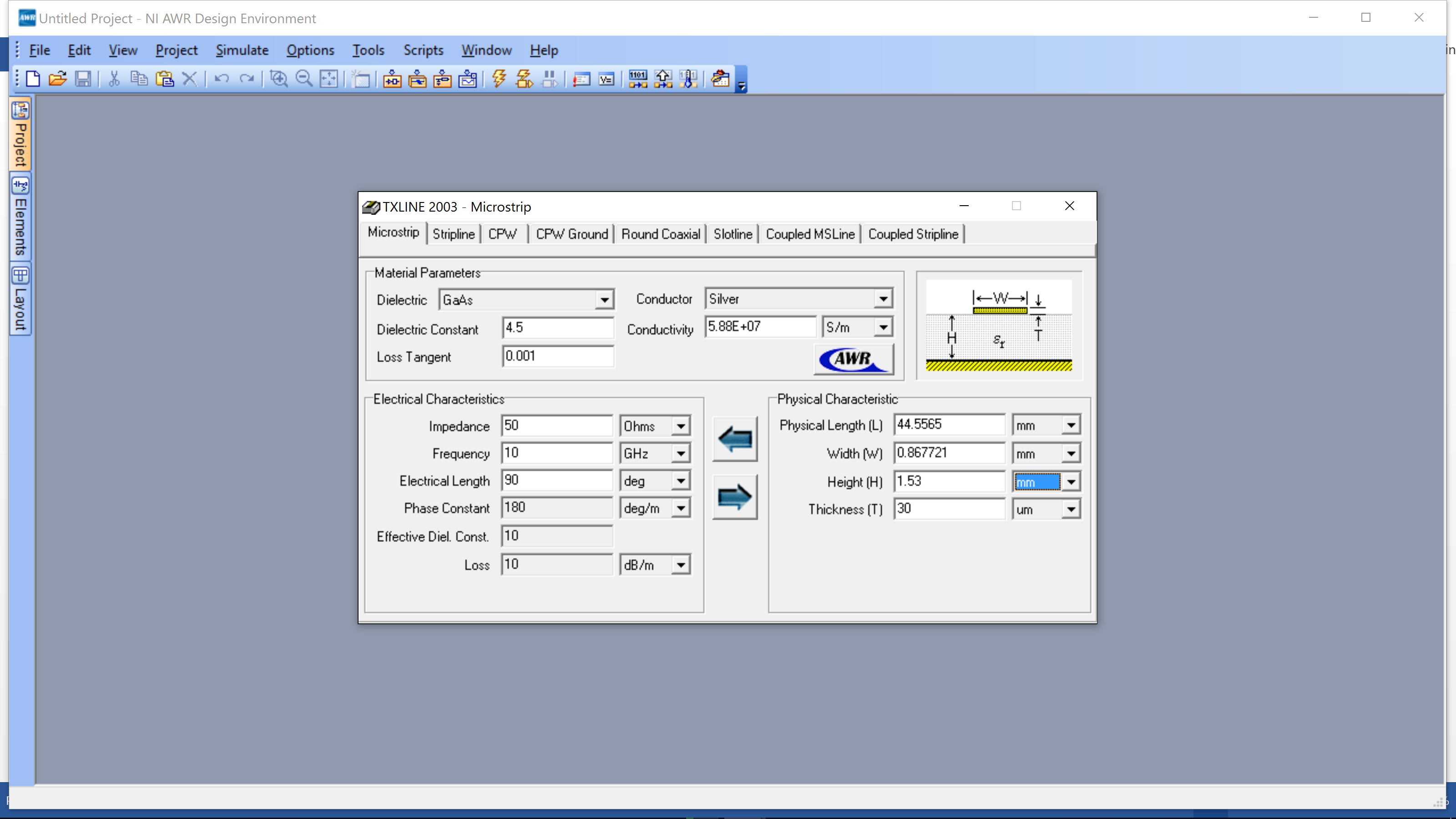
The picture shows a transmission line with a 50 Ohm impedance and an electrical length of 90 degrees at 950 MHz. The calculator works bidirectional. To find a transmission line from electrical length, insert all of the the parameters on the left. Also set Dielectric Constant=4.5, Conductor=Copper, Height=1.53 mm, Thickness=30um. These are obtained from the PCB stackup we are using in the workshop. Note that the Height and Thickness are set on the right side, even though we are calculating from left to right in this example. Click the right arrow – it will calculate the width and length to the line. Likewise, if you change the Length or Width on the right side and click the left arrow, it will calculate the new Electrical Length and Impedance.
The impedance transformation can be understood in this video and the characteristic impedance of the transmission line calculated as follows:
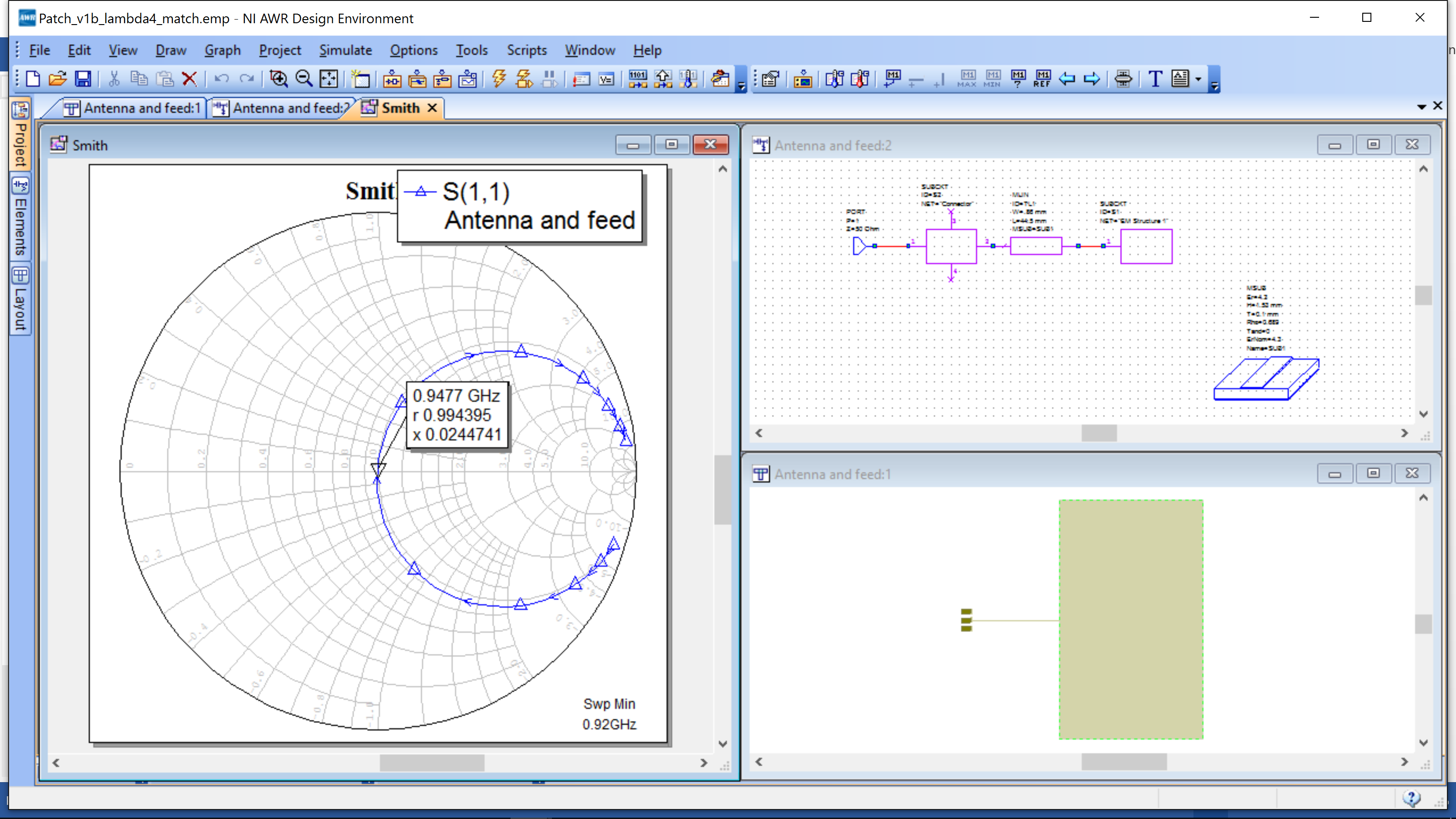
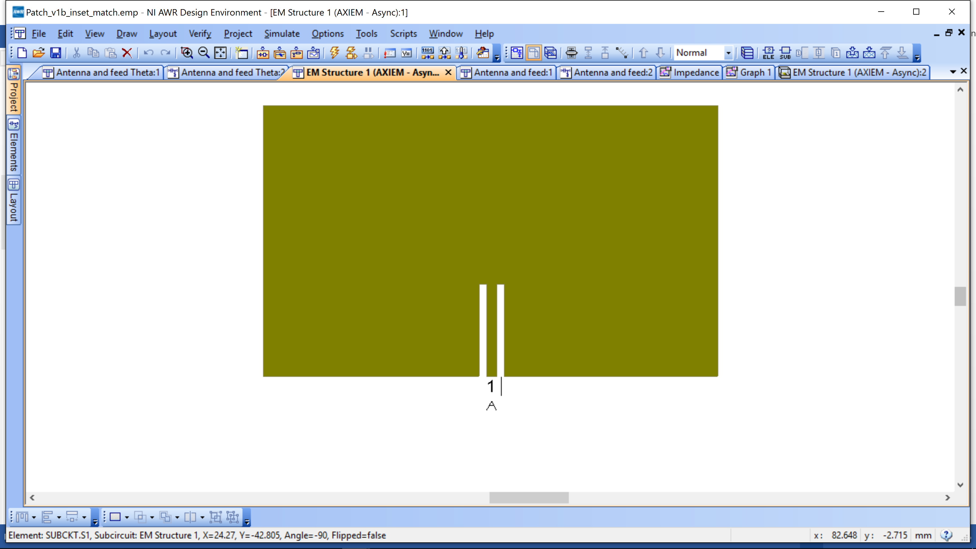
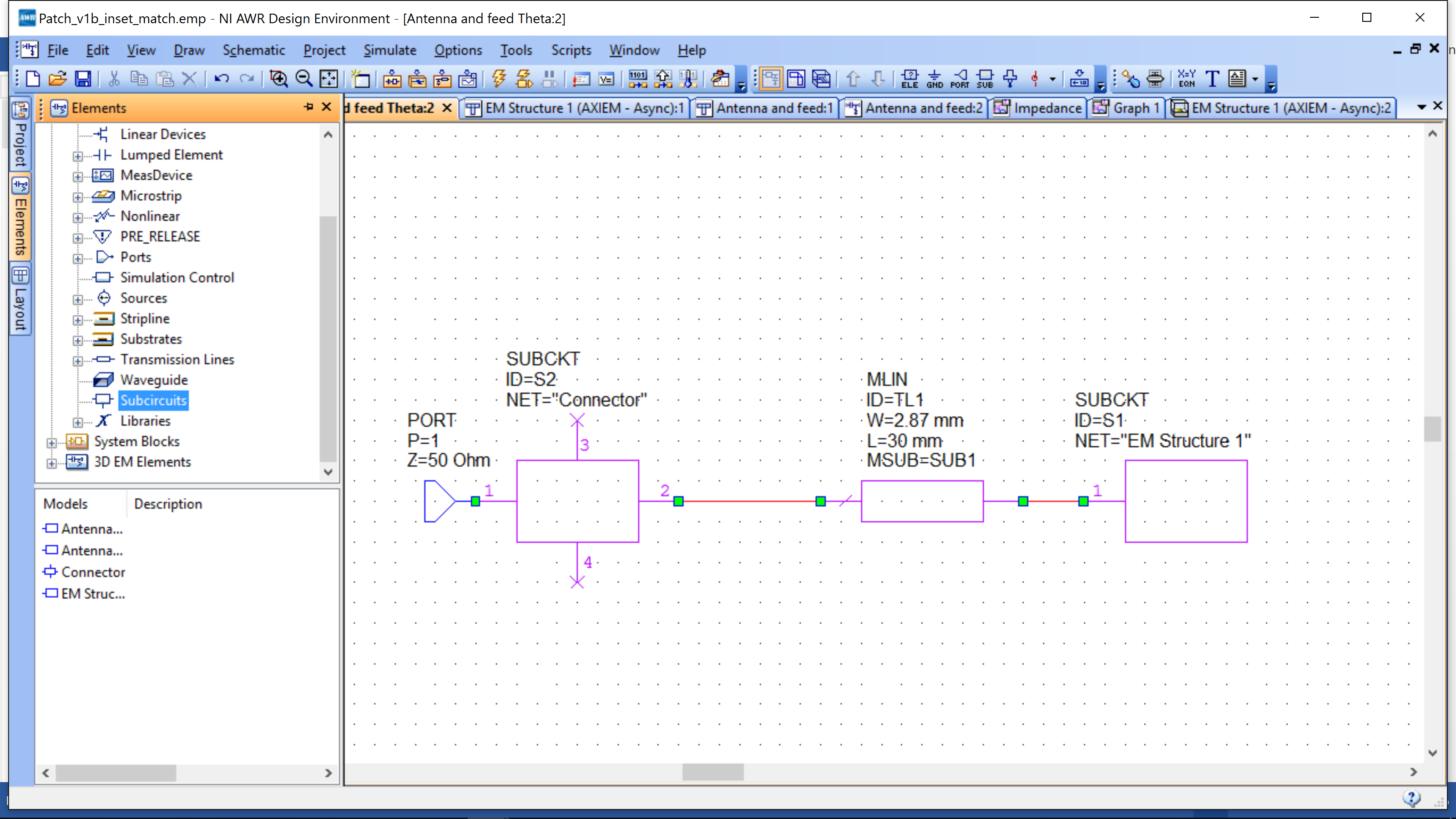
Create a new schematic and insert the patch from the Elements->Subscircuits->EM Structure 1. AWR/NI saves every design element with ports as a subcircuit. This subcircuit represents the EM layout of the patch. Now insert a MLIN with the correct length and width in mm from TXLINE and add a 50 ohm port. You can now simulate, using a Smith chart, the input impedance to the t-line.
Your schematic, layout and S11 should be similar to this figure below.
Antenna Pattern & Gain
The match at 50 Ohms suggests a good design, however the antenna should be simulated for the radiated pattern and antenna gain. Antenna gain is explained in this video.
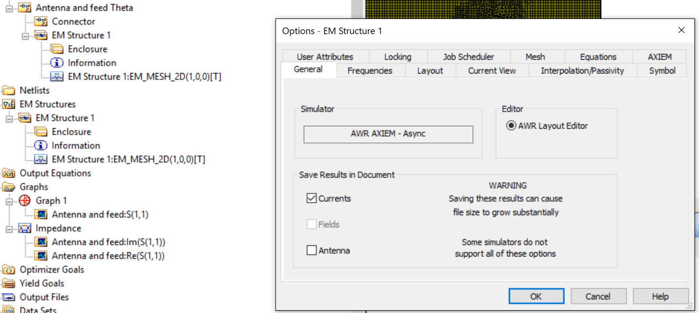
To see the field patterns, we need to run the simulation at a single frequency. The best way is to copy and paste the circuit schematics by right mouse clicking under the Project Tab->Circuit Schematics->Your Schematic Name and select Duplicated. You can then rename “My Patch_Patterns”.
Right mouse click on EM Structure under the new schematic you created and select Options at the top. You should see this window. Enable Currents – this will allow us to see the 3D pattern.
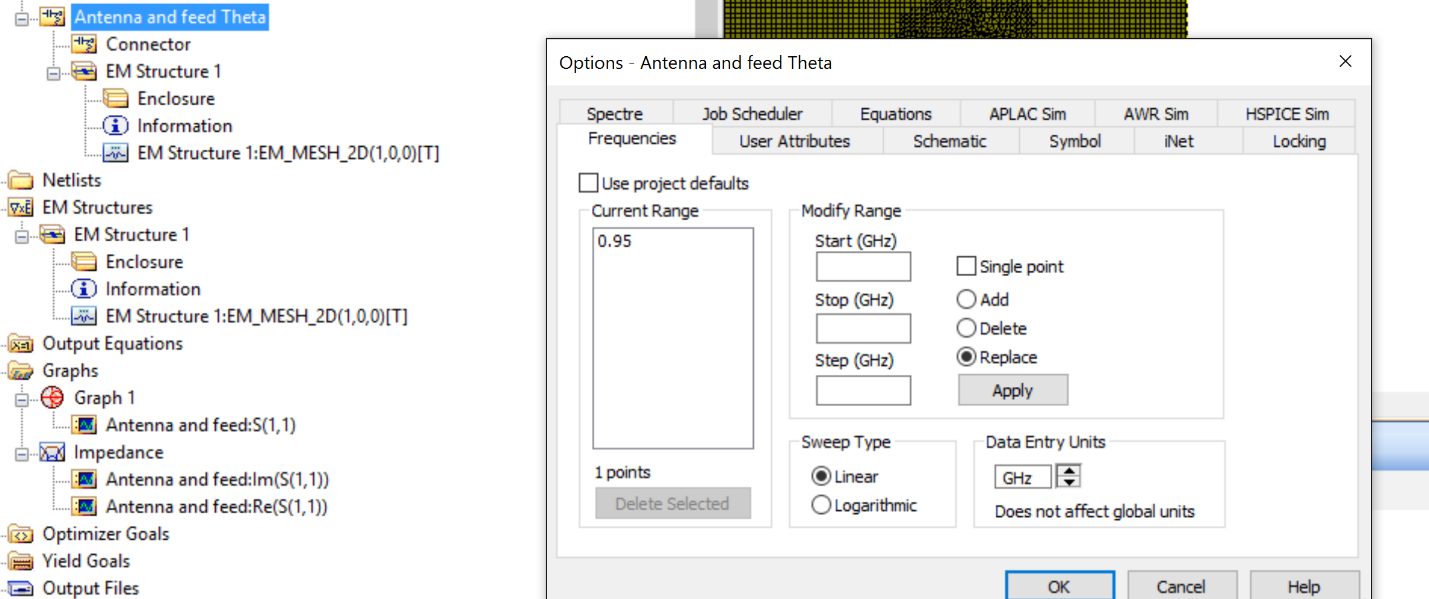
Now right mouse click on the schematic name under the Projects Tab->Circuit Schematics and select options. Under the Frequencies tab, unselect Use project defaults and set it as follows for a single frequency by selecting Single point.
Before plotting the field patterns, it is necessary to understand the coordinate system. Below is from the Meas Help button on the measurement window.
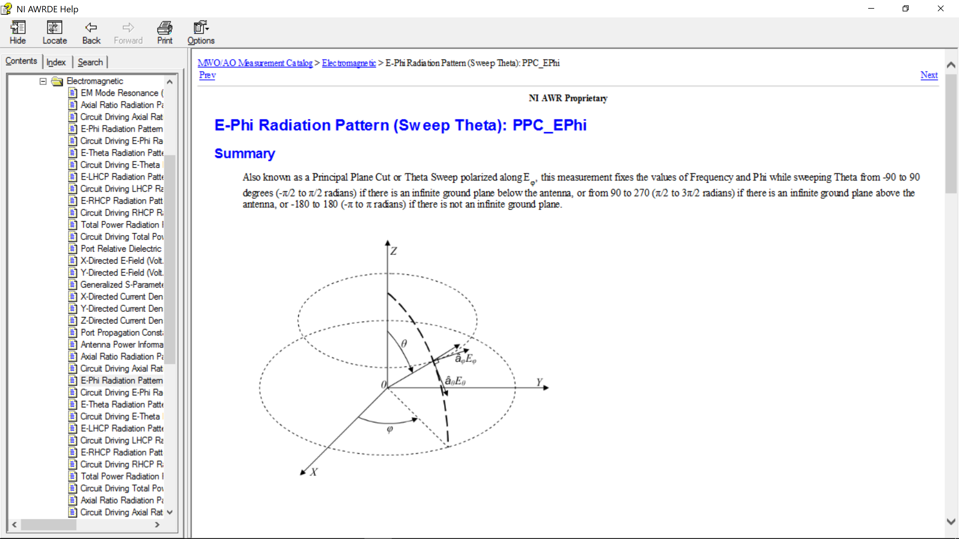
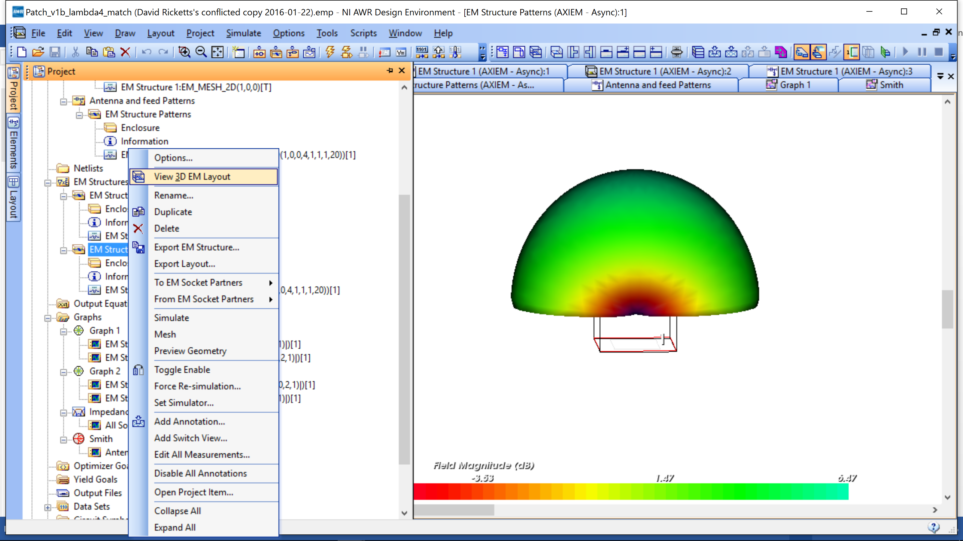
We can see that Phi is the angular direction in the X-Y plane and theta is the angle form the Z axis. We will plot the antenna pattern in the X-Y plane and the X-Z plane.
Below is a measurement of the X-Z plane as theta is swept.
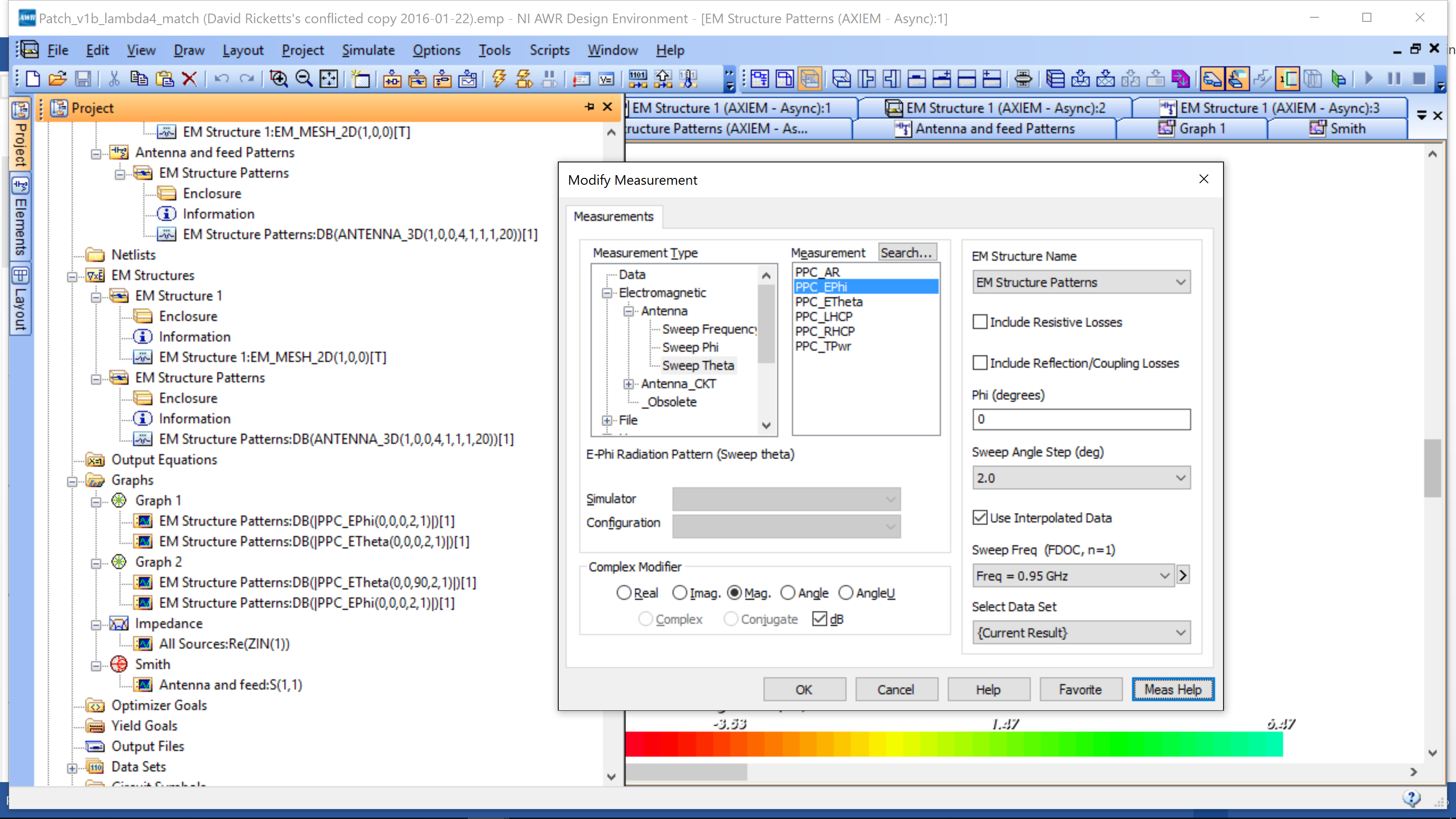
You can see that Phi=0, which is the X-Z plane and we have selected Sweep Theta. Select PPC_EPhi, hit OK, then add another measurement of PPB_EThetab. These plot the electric field in the Phi and Theta directions in the X-Z plane.
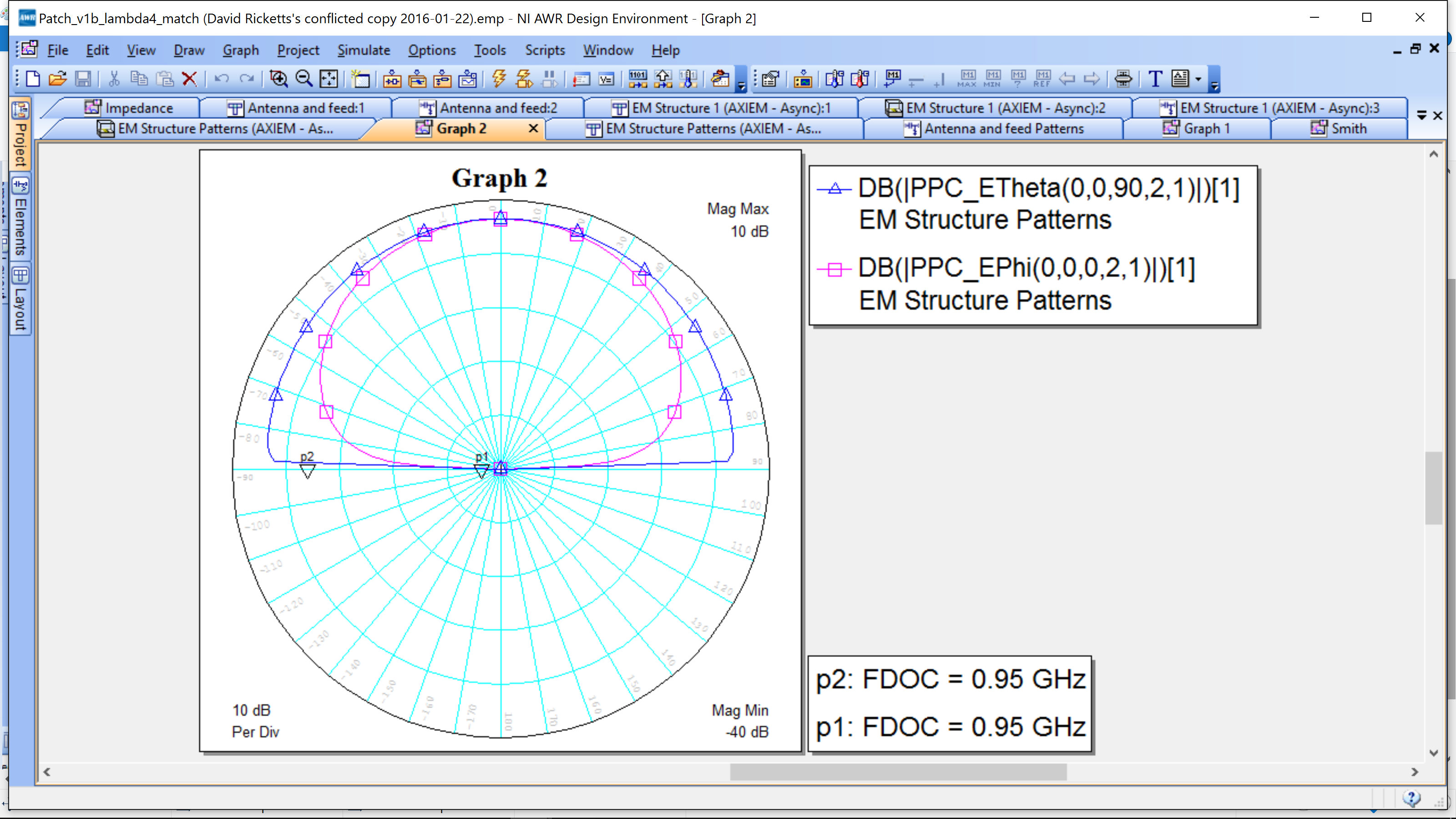
This shows that the peak fields are at Theta=0, which is directly above the center of the patch.
You can also plot the pattern in the X-Y plane, however due to symmetry this is not as interesting.
To plot the 3D fields, simply go to the layout and select as below. The 3D pattern will now show. You can use the view tools to rotate by simply clicking on the pattern and moving your mouse ( it will rotate in response).
Impedance matching II – Inset T-Line
Another impedance matching technique is to use a 50 ohm transmission line and cut “insets” out of the antenna. Below is an example layout.
The length (along the T-line) and the width of the cutout can be calculated using the following equations.
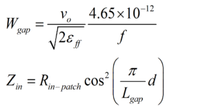
It can be seen that the impedance transformation from the patch to the 50 ohm T-line is proportional to cosine2. The input impedance starts at Rin-patch and goes towards zero. This is a good method for tuning after you run your simulation. The imaginary part of the impedance will be determined by the patch and the size of the gap – you can play around with sizing to see if you can zero it out!
The gap can be created by copying the square and reducing it size to the size of your calculations. Then place it where you would like the gap – you’ll need two copies, one on either side of the transmission line. The transmission line is made by simply leaving 2.3mm wide metallic piece between the two gaps – you do not add anything at this point. With your two rectangles placed on top of the antenna, you can us Draw->Modify Shapes -> Subtract. This will subtract the rectangles you just made from the rectangular patch. It is context sensitive – meaning what you select first – the patch or the rectangle, will determine what gets subtracted from what. Once you hae done this, you can double click the new shape and you will see blue points on the new gaps. From this point, you can just adjust those as you see fit.
You can now add a 50 Ohm transmission line to connect to your 2.3mm metallic piece that is between the two gaps and add a port at the end. Note that now the length of this feedline is not dependant on the impedance transformation.
You may rerun all of the plots above – they will look similar. You can adjust the gap size to try to enhance the match.
Layout
Finally you want to make the fabrication layout of your antenna. The design is already there, you just need to add the connectors. While the Schematic view is active, select the Elements Tab in your project browser, and under Subcircuit, select connector and add it to your schematic. The figure below shows the connector and sub
You will notice that the schematic symbol of connector has four ports. Port1 will be connected to the simulation port, Port2 will be connected to your coupler, and Port3 and Port4 can be left open. Add this subcircuit to all the four ports of your coupler.
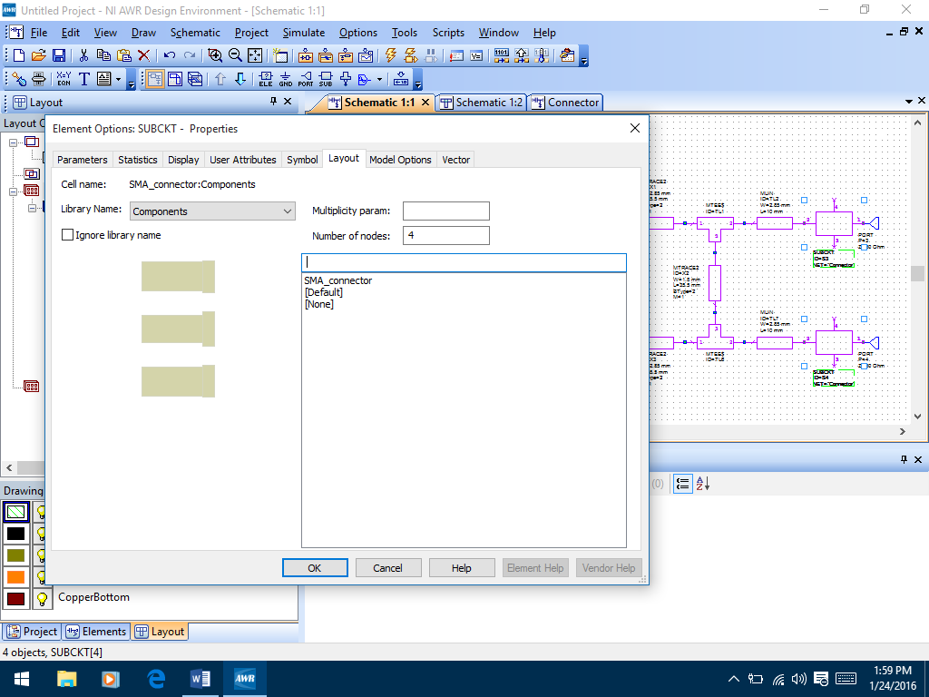
Now select all the instance of the subcircuit “connector” you just placed, right-click and in the properties>layout use the SMA_connector footprint. Make sure the library name Components is selected.
After this you can open the layout view, and the connector pads are added!
Fabrication
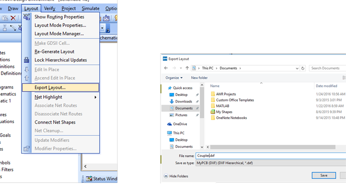
To fabricate, print out your antenna layout on a sheet of paper, making sure it is the correct dimensions (check scaling options when printing). You will transfer to a copper foil and cut out the antenna by hand. You can also export this layout to a DXF file for printing if you would prefer to print a .dxf and have the software to print a .dxf.
Testing
For the workshop, simply connect Port 1 of the VNA and measure S11 to see where the antenna is centered. If a friend has an antenna, you can connect that to Port 2 of the VNA and meausre S21.
Antenna Theory Videos
The following are informative and in some cases fun to watch.
