Fabrication – Assembly
Assembly
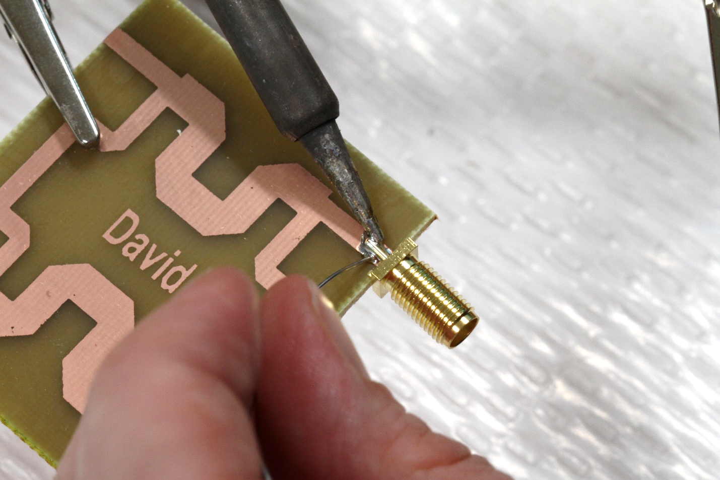
Each design document has directions on which components are soldered where. SMA connectors are soldered directly on 50 Ohm transmission lines.
The following we review basic soldering techniques for surface mount devices (SMD) and a few tricks for the difficulty SMD components included in the kit, such as the inductors and baluns, which only have pads on the bottom of the part.
SMA Connectors
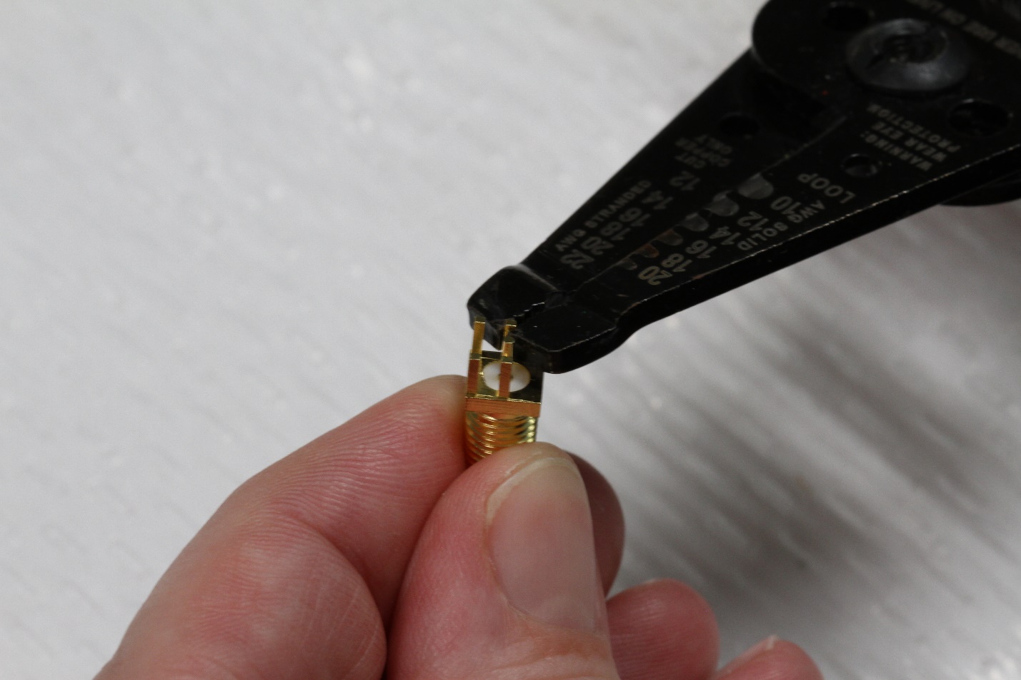
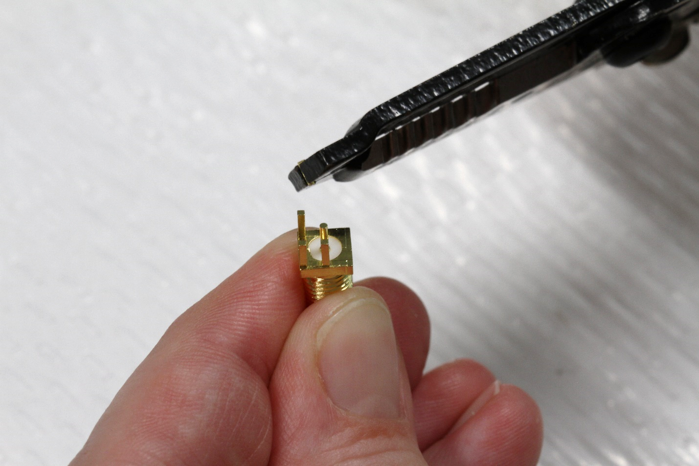
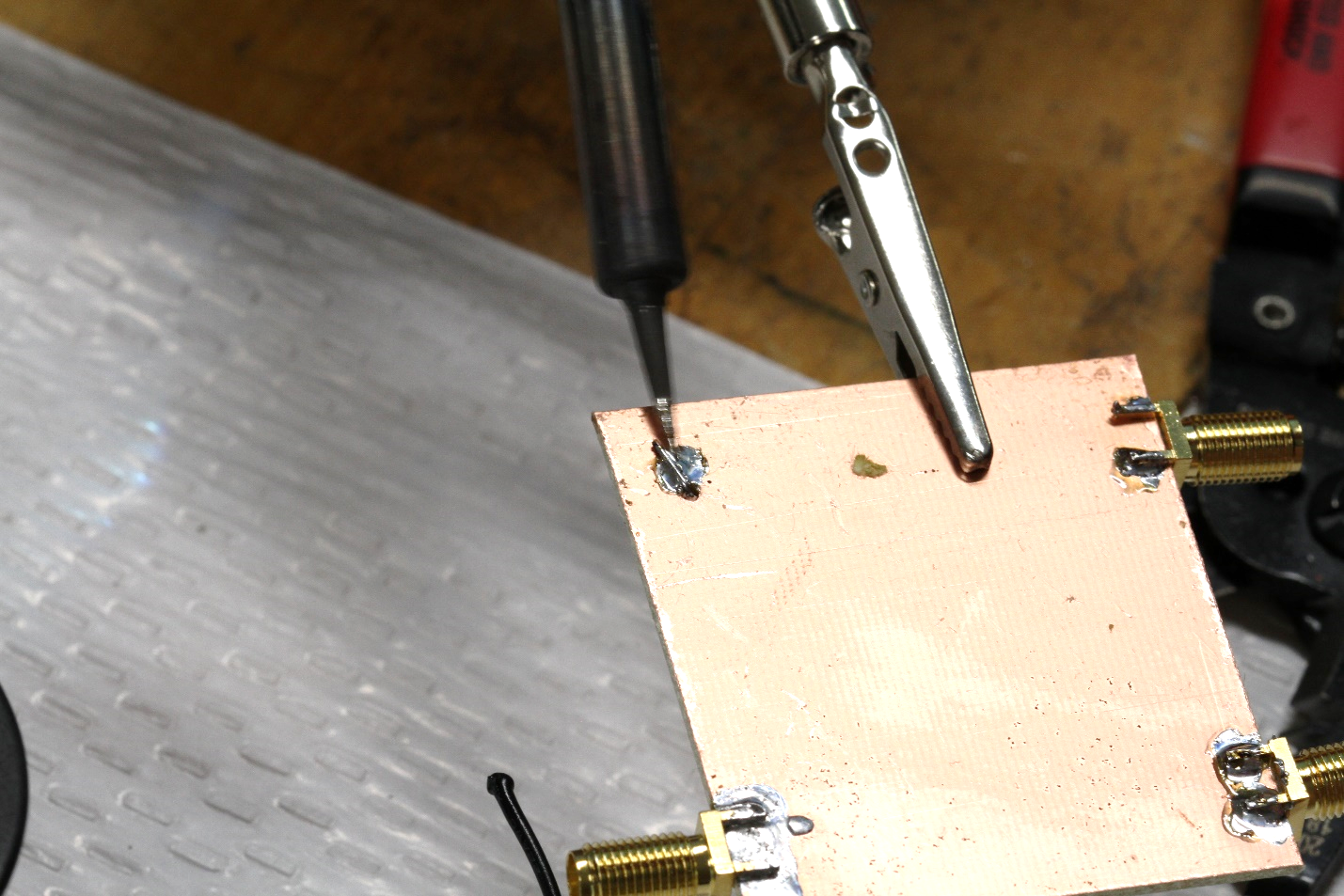
The SMA connectors are soldered directly onto the 50 Ohm transmission lines you added to each design. Due to the size of our connectors, it is difficult to space the ground pins away from the transmission line. We therefore recommend removing them.
Please wear eye protection and be aware of anyone around you without eye projection – move to a location without other people or have others put on eye protection also.
Using the tip of a needle-nose plier or wire cutter, gently break-off the top feed of the SMA connector. The top pins are aligned with the center conductor. The bottom pins will be soldered to the back of the PCB.
Soldering
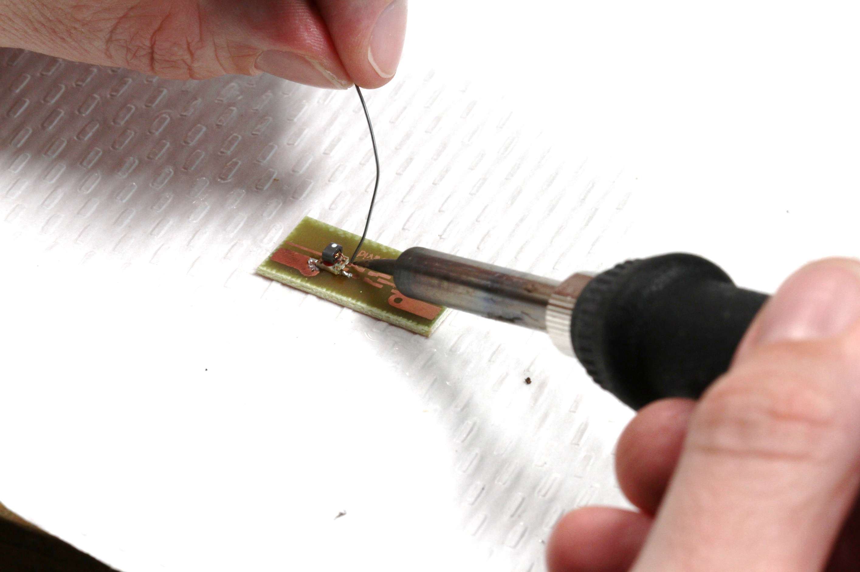
Soldering is simply the use of a low-temperature metal to connect two electrical terminals. The key to a quality connection is: cleanliness (no oil or oxide) and appropriate temperature on all terminals. The PCBs that have just been etched are very clean. It is therefore only needed that you heat all parts to be soldered.
Set the soldering iron to 350 degrees.
Below is an example of an SMA connector (top pins removed) being soldered onto a board. Note that the soldering iron on the top side and the solder is on the bottom. The iron is used to heat the trace and pin fully, until the solder melts. By doing this, both the pin and trace will be at the correct temperature.
Often, an inexperienced person will place the solder on the iron to melt it and then will try to touch the terminals with the melted solder. This approach sometimes works, but does not ensure all terminals/traces are at the correct temperature (the only method to see that the temperature is correct is to see the solder melt on the terminal directly). When both terminals/traces are not at the correct temperature, a “cold” solder joint will occur. This when the solder adheres to one piece, but not the other since it is not hot enough. This is very common on the ground plane of PCBs.
Below is a picture where solder was heated by the tip and then placed on the PCB ground. Note it does not “wick” out or did not “flow” out on the PCB. This is because the PCB is too cold and the solder does not adhere. On the right is the same solder after the board is heated by the soldering iron more. You can see that is “flows” out and “wicks” to the terminal of the SMA.
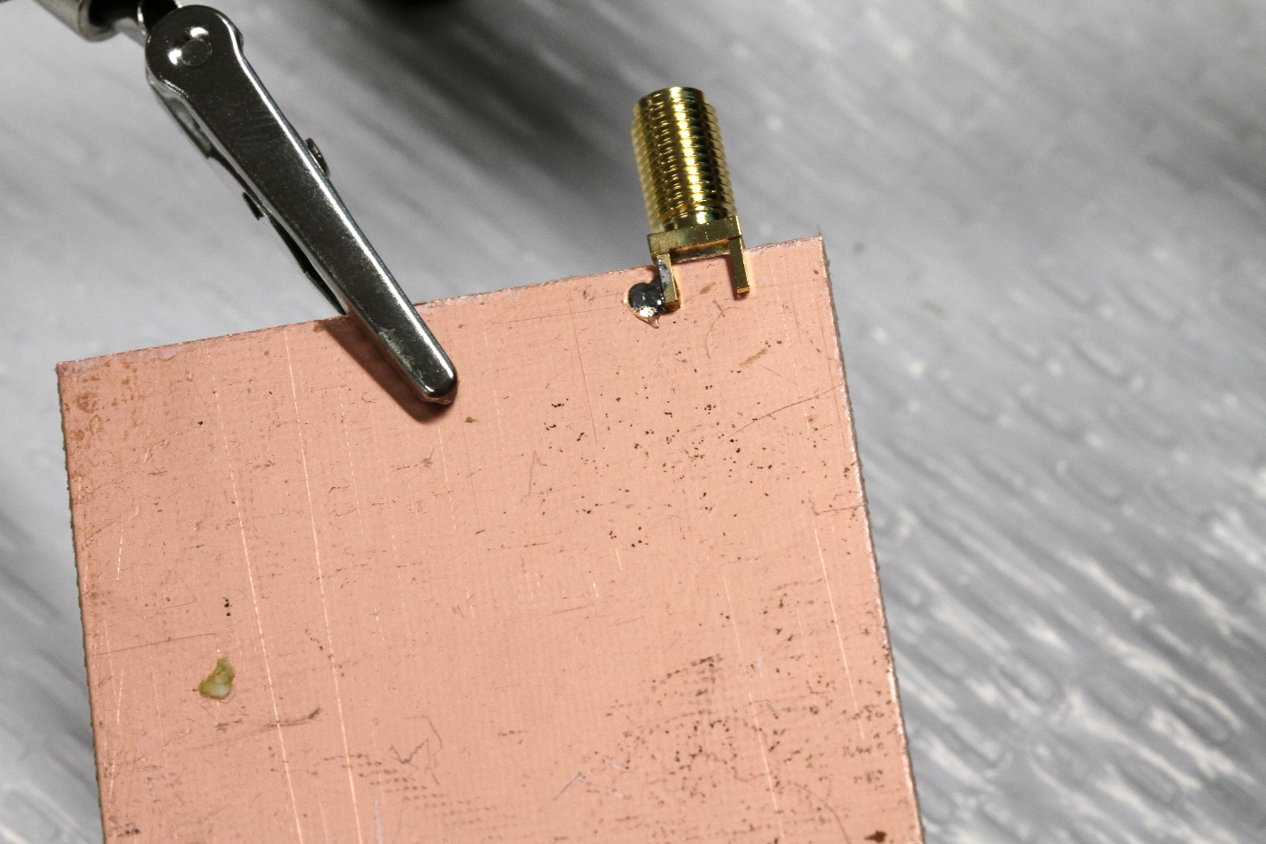
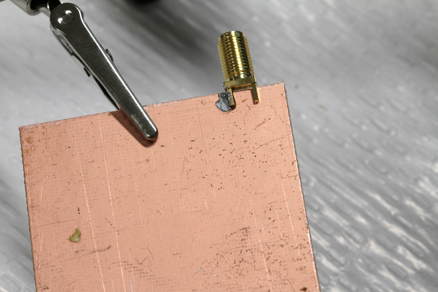
The SMA ground plane connection is the #1 cause of non-functional parts in the workshop as the large area of copper requires significant heat, and many new participants do not heat the board enough.
Make sure your solder joints are not “cold”!
Vias
Our simple fabrication process does not have a through via to connect the top copper to the ground plane, so we use a simple wire.
Drill the via hole with a 1/16” or 1.5mm drill bit. Place the PCB on a firm structure. table.
Make sure:
- The underside of the via is off the table – make sure not to drill into the table!
- The board is held securely – the weight/pressure of the drill should not tip the PCB
- Your hand is not underneath the via hole!!
- Wear eye-protection.
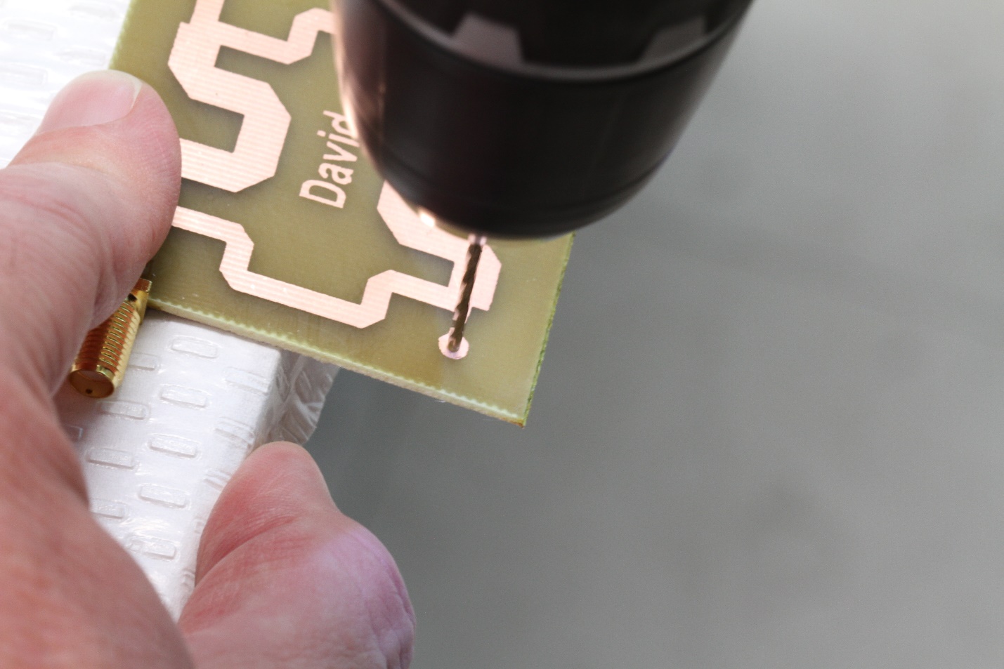
The via is made by taking a small piece of stripped (no insulation) solid 22 AWG wire and placing it in the hole and soldering the top and bottom (make sure there are cold solder joints on the bottom).
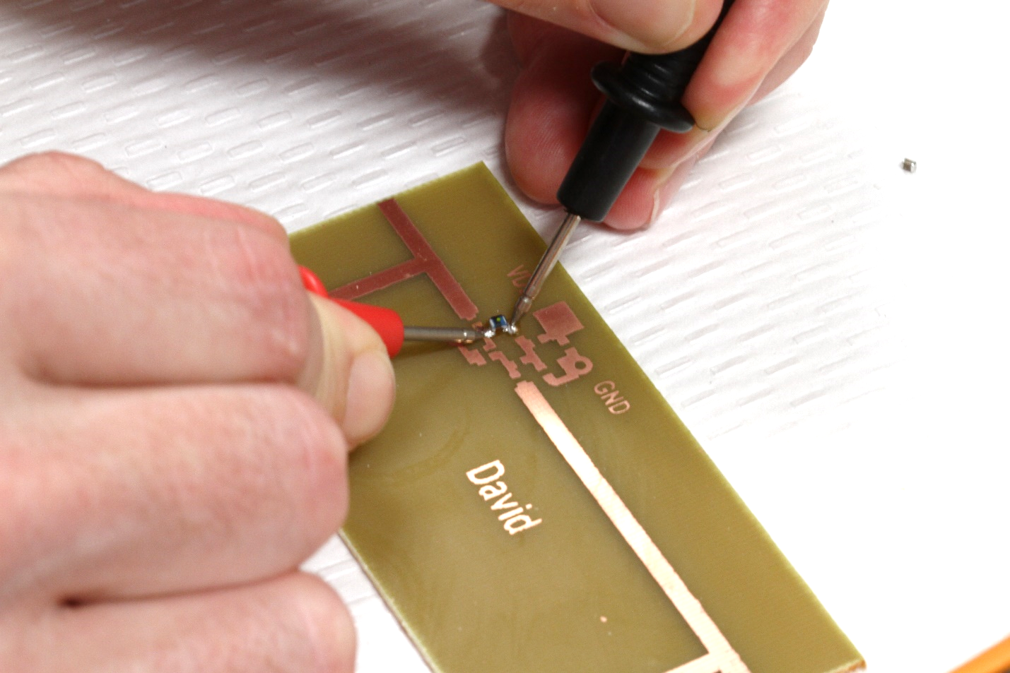
Soldering SMD Components
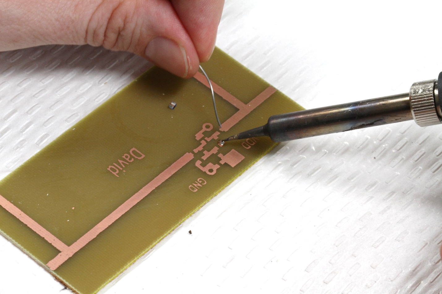
We will demonstrate a quick and easy way to solder SMD components using the SMD inductor as an example. The Inductor is challenging as it only has a pad on the bottom of the part, there is nothing to touch the soldering iron to on the side. This is OK, as in a good soldering technique, we should be heating the copper trace not the part (the solder will heat the part, as it has a very small thermal mass).
Placing solder on bare copper is called “tinning”. It is generally done on the ends of wires, but we will re-use the term here for our PCB. “Tin” one side of the pad where you wish to place your part. Place the soldering iron on the copper trace, then place the solder on the trace direction (not on the iron). This ensures good adhesion of the solder. There should be a small “pool” or extra amount of solder.
Now using a pair of tweezers, place the inductor on top of the tinned pad. Using the soldering iron, heat the copper next the inductor. The solder on the trace will melt and will “wick” to the underside pad of the inductor. Due to the small size of the inductor, the solder will heat the pad enough to make a good solder joint. This will not only solder one terminal of the inductor but physically hold the SMD part in place as you solder the other side.
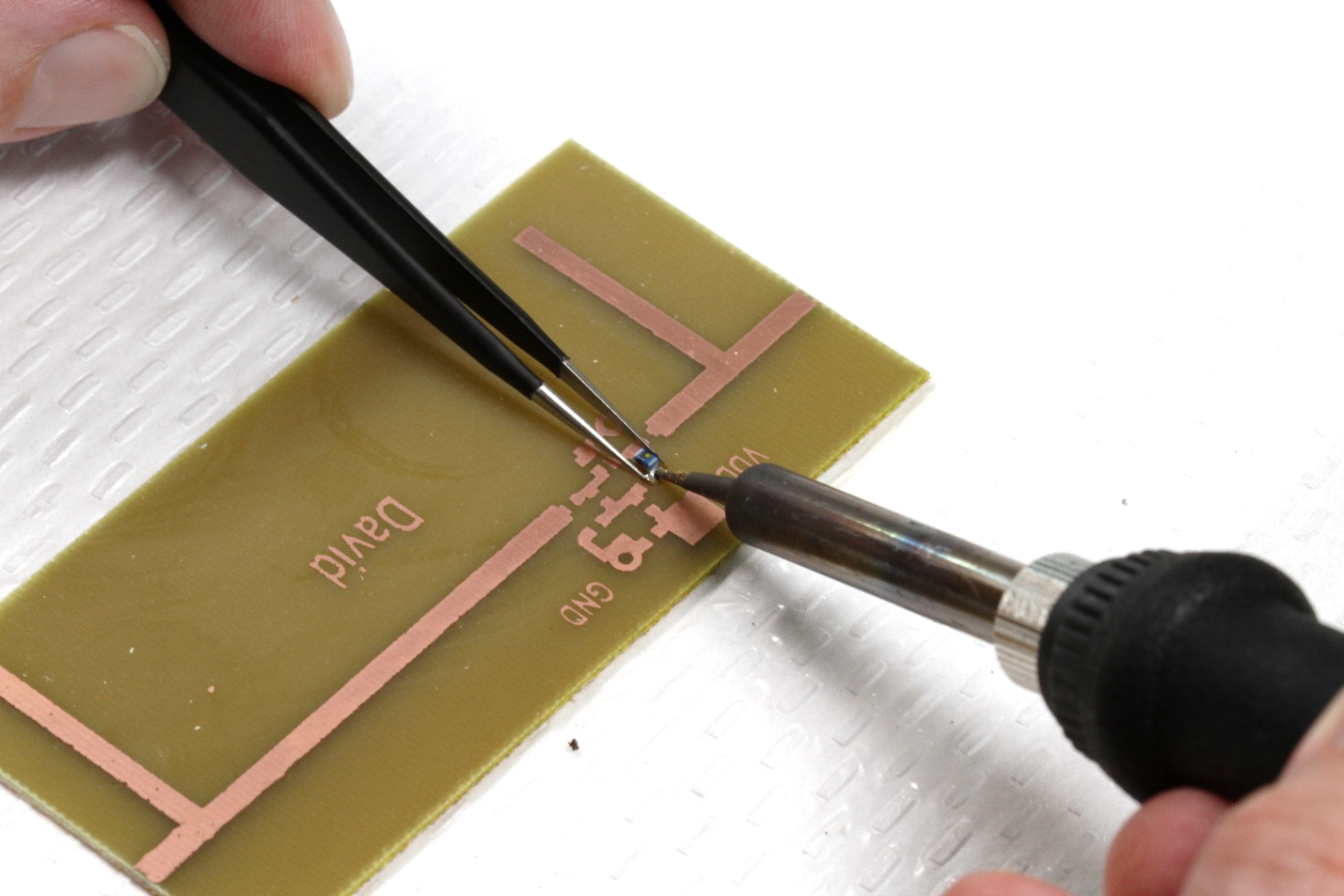
You can now repeat the other pad, heating the trace then applying the solder until it wicks under the part. You should go back to the original pad and re-heat it to make sure the solder joint is good, adding additional solder if needed.
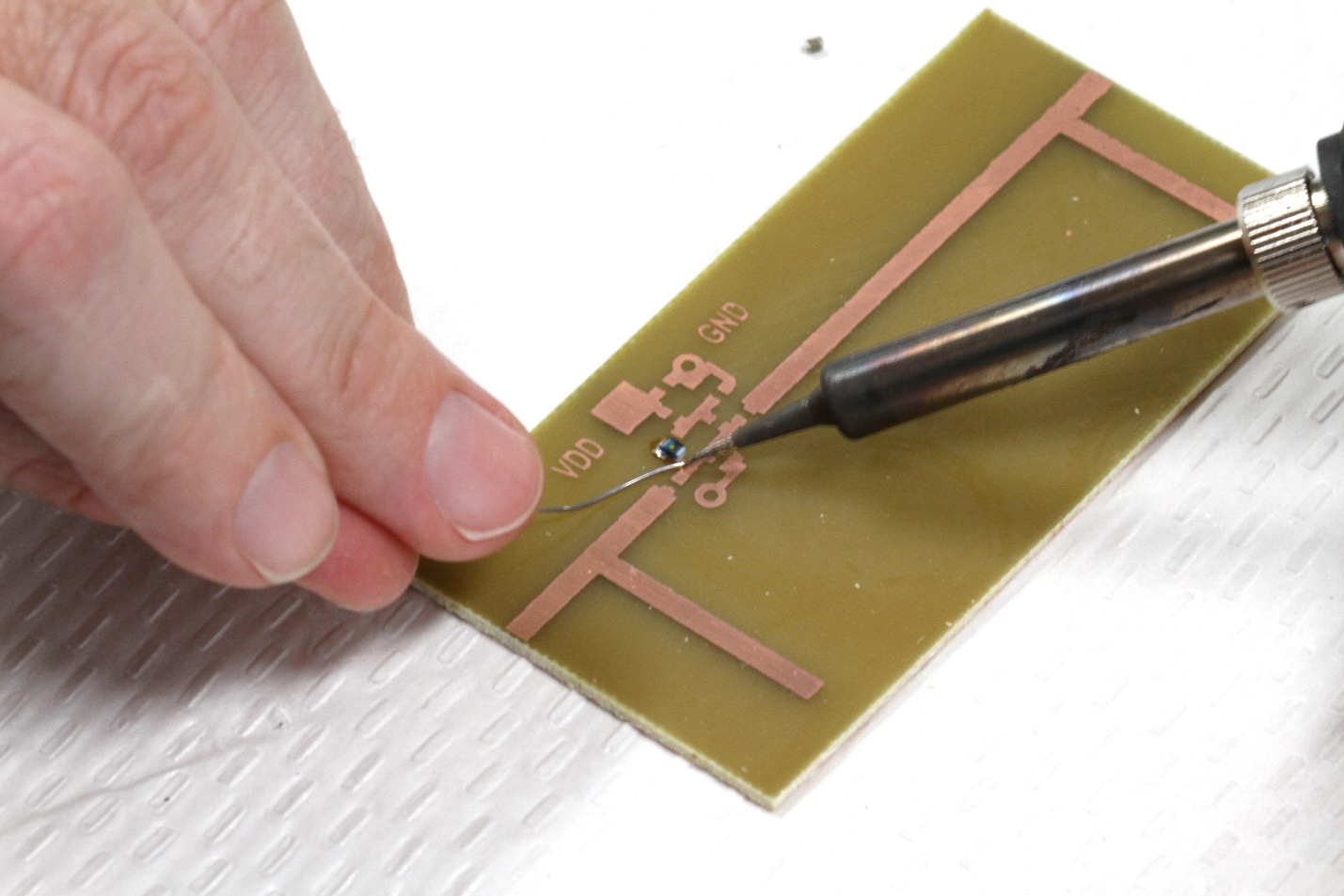
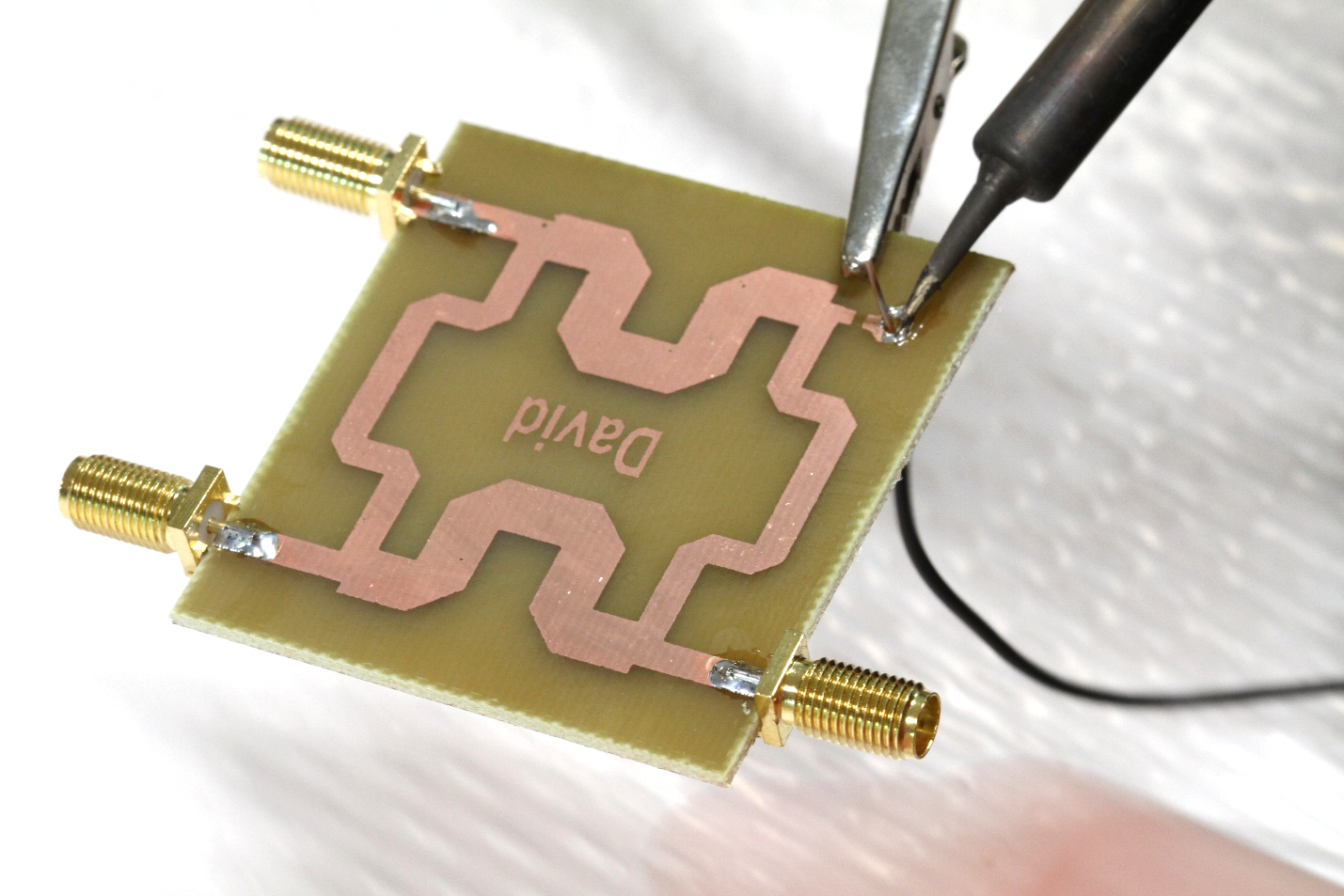
It is a good idea for parts that does not have visible pads (inductors and baluns) to check the connection with an Ohm meter (many meters also measure diodes, which is convenient for diode and BJT connections). The inductors should measure 0.5 Ohms; other components should measure according to their value.
Soldering Baluns
The baluns for the mixer are one of the most difficult parts to solder as they have 5 non-visable pads on the bottom. Using the technique above for the inductor, you can solder the baluns easily.
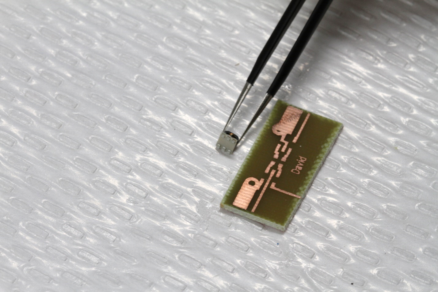
The following images show the process. Note that the balun has 6 pads, one side has all three connected to wires (center tap) and the other has only two connections (center pad is not connected to a wire). By using the circuit schematic and the layout, it should be clear which side of the balun is to be soldered (3 traces means the three wire side).
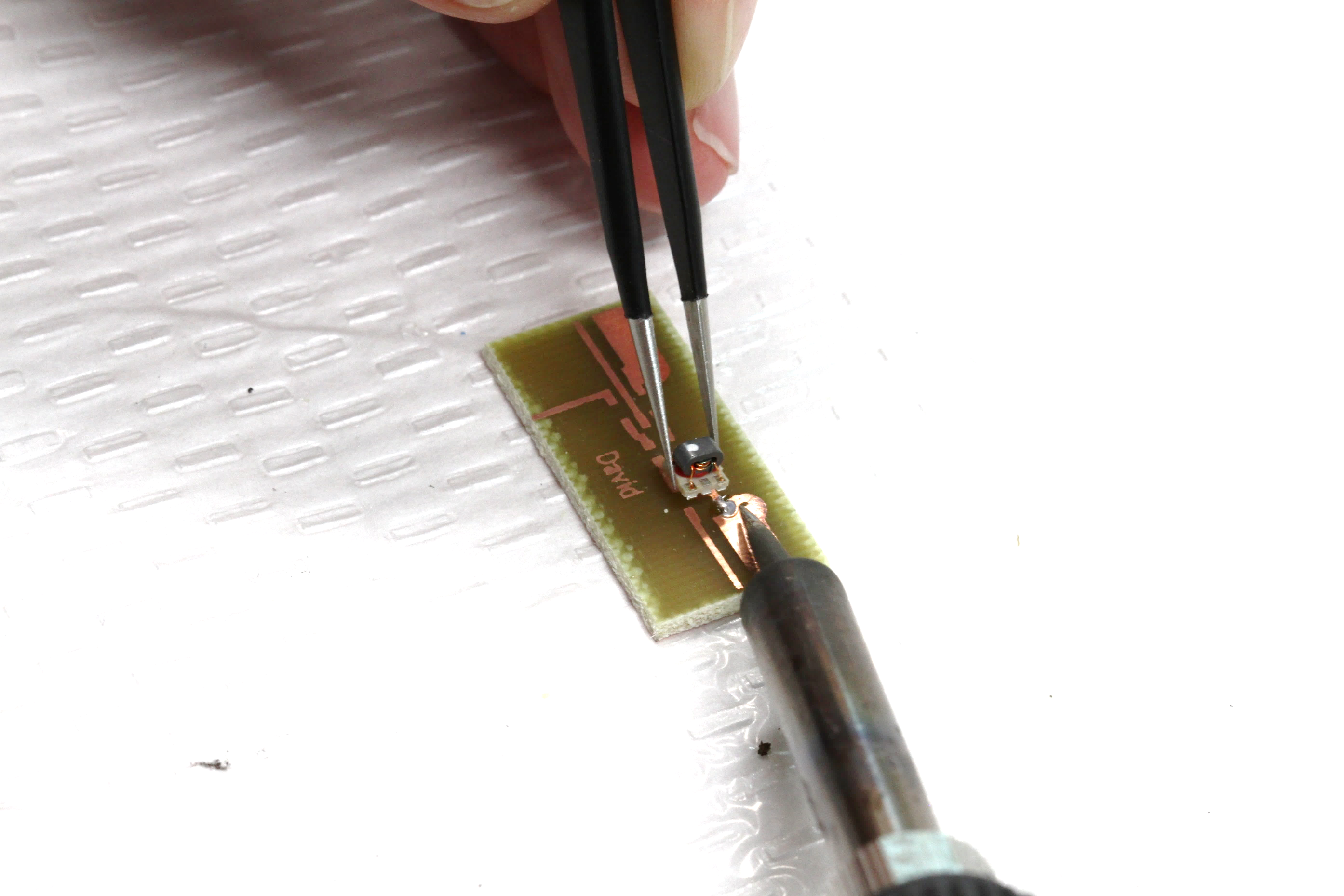
Rotating part to solder other side.