950 MHz Patch Antenna
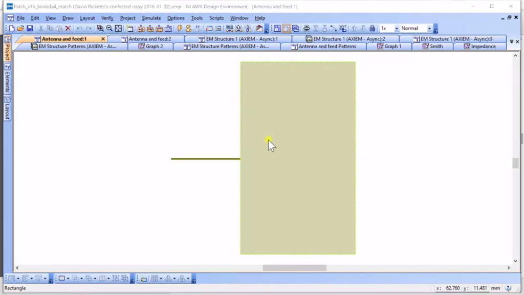
Welcome to our module in building the Patch Antenna. This is the antenna we’re going to build today. And you can see it consists of a patch on the right, and then an impedance matching transmission line on the left. This transmission line is not 50 ohms, but it’s actually impedance matching the patch antenna to what would be our port. Now if you remember from the design document, the width of the patch antenna is probably or is approximately a half of wavelength of λ/2. The length is also λ/2, but remember, we have to reduce the length to the fringing field in order to get the current electrical length. So, what should you do is you should go ahead and open your document and that is going to be titled “Patch Start”.
And what we have here is – I’ll actually walk you through this. So, if you look under “Project”, we have nothing in Global Definition on this one, which is just fine. And what we have our EM structures; so, our EM structure is basically a layout that the EM Simulator sees. So, it’s not under the system diagrams, which would be DSS and Doing System Simulations, and it’s not yet under Circuit Schematics. It’s just a single, electromagnetic element and in here, we have one structure and let me see if I can double-click here…
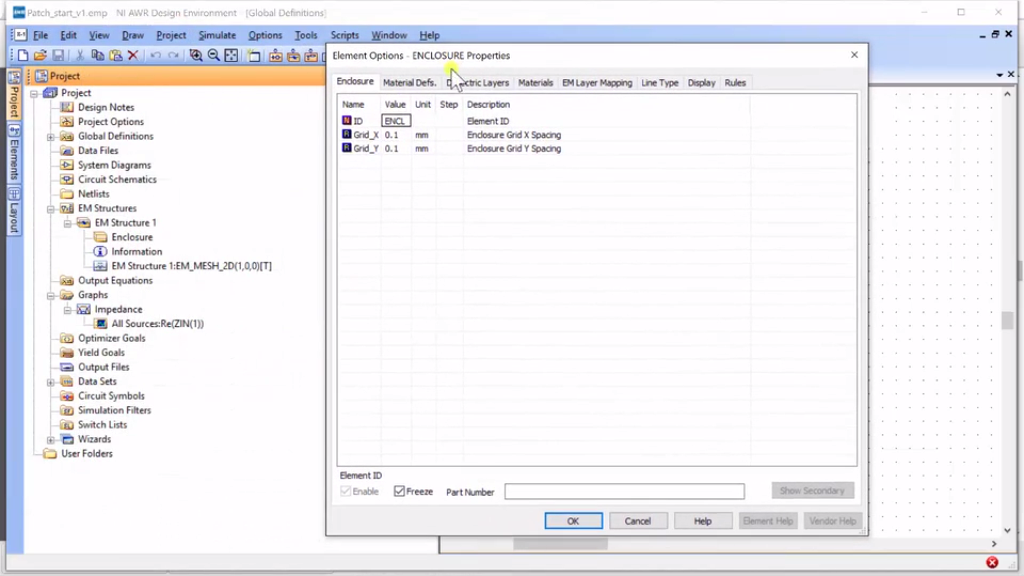
This is the enclosure and the enclosure represents the space around the antenna and I’ll just walk you through this really quick. We’re saying that the grid is on 0.1 millimeter spacing. This is important for the enclosure because it will try to simulate everything over the space. So, the larger this number is, the fewer the points in a given area, and therefore, the quicker the simulation.
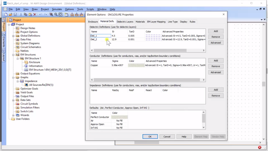
We’ve defined the materials, we’ve got our first dielectric, which has the dielectric constant of 4.5, we’ve selected a conductor called “Copper”, and the software already knows the properties insides. So, this is just a finding the materials. So, we could have a hundred materials here.
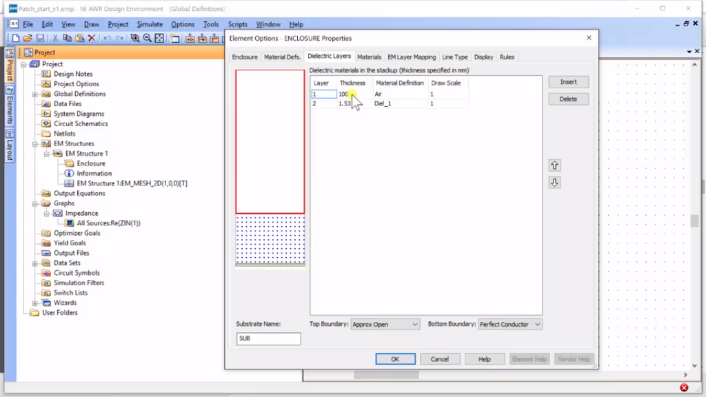
It would not affect our design unless we actually use them and so, if we look at our stack-up, this is our enclosure, if you will, in our RF space. So, we have an enclosure here that has the height of a hundred millimeters, and it is made out of air. We could pick any material. Here are the two dielectrics that we saw before, and then we have a second layer, which is our cord. So, the thickness of this is 1.53 millimeters, and that matches our F4. We’ve selected dielectric 1 because dielectric 1 has the properties of our material. And a quick thing to notice is that you’ll see on the bottom, this has a little kind of goldish brown bar. We set the boundary as a perfect conductor and this is just going to represent our ground plane. We want more accurate simulations. We’re probably going to do 3D simulator and you can actually make that copper. We go look at the top for the air and you’ll notice that the top boundary is in approximate open. So, we’re basically saying that this is free air going about.
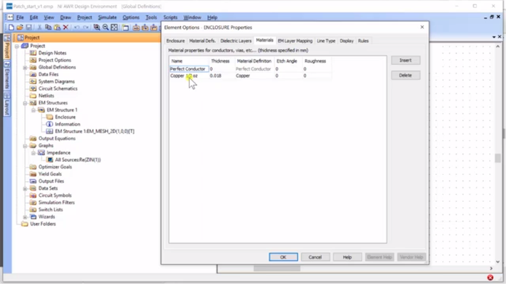
So, let’s just go look through the rest of this. So, I’ve defined a metal layer called “Copper Half Ounce” and the thickness is 18 microns. And that material is copper and that material goes back to material definitions, then yeah, it’s right there.

And if I go to our EM material layer, “Copper Top” is EM Layer 2 and if you’re wondering, you could just go back here to “Material Definitions” and here we go to Layer 2. The Copper Top goes on top there and this is perfect. We don’t have any VS, so we don’t have to worry about checking anything there. And the line type basically when we draw things. This is the line and we’re going to draw and it’s going to be made out of material copper 1/2 and here are just a few more metrics or options for us. And that goes over the element options.
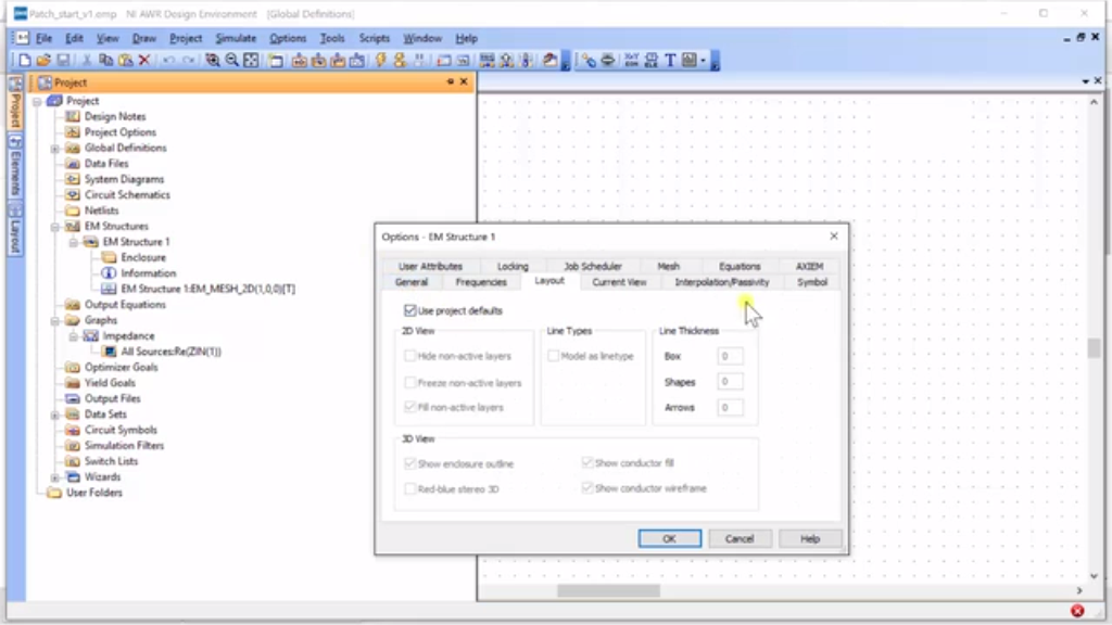
And let’s just look at the EM structure. Let’s hit “Options” here. And this is just some general aspects for the simulator. And if we go to here, we can see the options for the frequency range. We could click “Project Defaults”, which works fine. We pre-set 0.92 to 0.98; you may find that when you do your simulation, you need to make this much larger in case your size is not accurate. Basically, what I do is I search from about 0.5 to 1.5 gigahertz to find where this center is and tune my patch to around 0.95 or 950 megahertz, and then you can narrow the range. If you look at the design document later on, there is going to be a time where you plot the fields and when you plot the fields, you only want to do it at a single frequency and in which case, you could copy and paste or duplicate a structure and then change your frequency here on this graph.
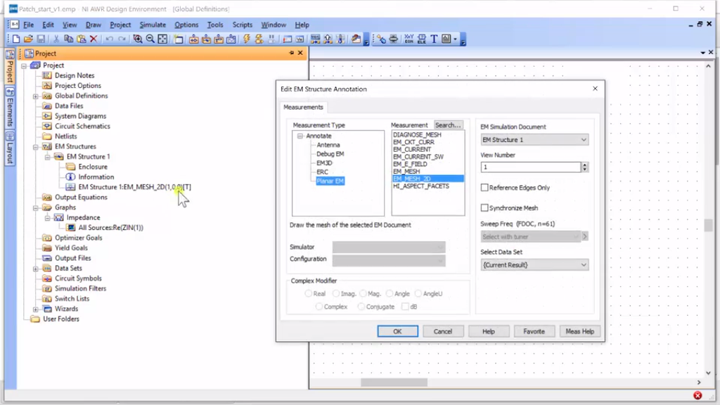
Finally, let’s just look at the top, and this just has a little bit more of general aspects of the layout. So, I’ll double-click this and this is actually just a mesh of our device and I’ll show that in just a second and I’m just going to show you the final one.
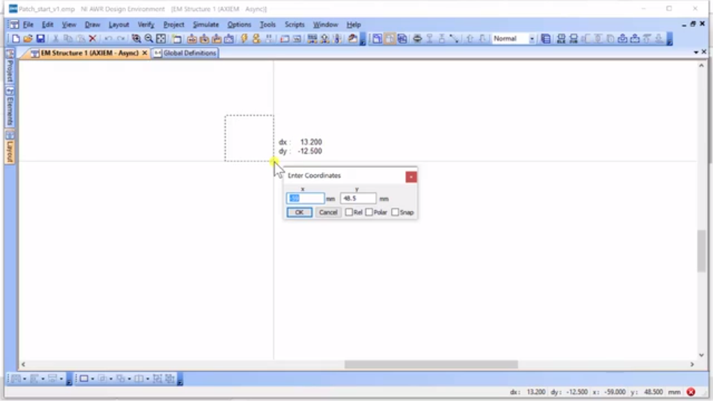
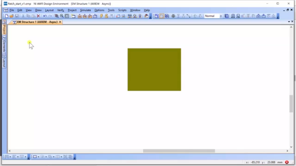
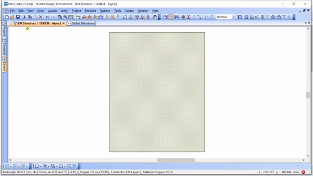
Alright, I want to show you how to create your rectangle and I’m going to click it and hit “Delete” and then I’m going to draw a square and if you start drawing a square and you hit the space bar, it’s going to allow you to hit the coordinates and this is really helpful for entering an initial square and it does it by XY, so I’m just going to hit a hundred. X is going to be along this way which in our previous diagram, that would have been our length. So, we’re going to make that a little bit less and we’ll make that 80 and I’ll make the Y dimension 100. These are not so far-off from our design values, but certainly not the correct one. So, click “Okay” and then if you hit Ctrl and the center mouse pad, if your computer has that, it would allow you to scroll out. And so, we can see here it has created a 150 line and if you’re wondering why is that? Well, that is because I added the X component and the Y component, we’re actually absolute and let’s select this, delete, and let’s go back and try that again.
I hit the space bar and I’m going to hit “Relative”. Now, it’s going to give me DX and DY, which are just the dimensions of the change. So, our X is our effective length, and we’ll do 80, and Y is our effective width and we’ll do 100, and then, there we go. And once again, I’m just scrolling with the center of the mouse hitting the Ctrl key or you could just do “Zoom Out”, okay.
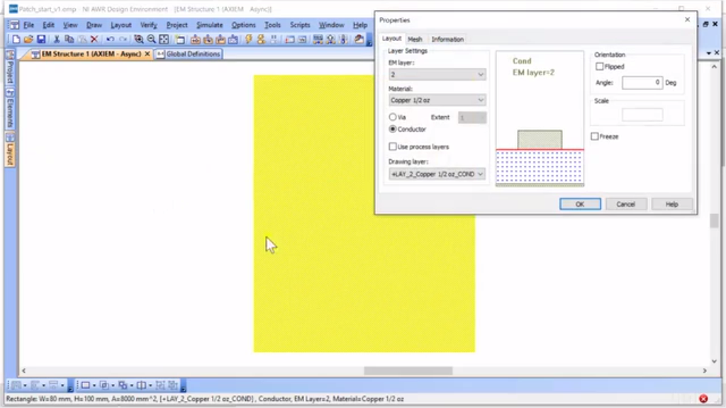
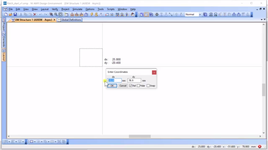
So, the question is what material is this? Well, I can go to “Shape Properties” and what I want is EM layer 2, I show it right here, Copper 1/2, okay; that’s great and so there I am. So now, I have my copper, and now what I want to do is I want to measure the input impedance of this. Let me understand where I am in context to resonance. So, what we’re going to do is we’re going to create another shape and I am just going to call this, hit the space bar, and for the X, I’m going to make a 0.1 millimeter and for the Y, I’m going to make a 0.3 millimeters. Why am I doing this? It’s because 2.3 is roughly a 50-ohm transmission line and 1.1 is just a small enough piece that it would give me what I don’t need at all. I’ll show that here in just a second.
There’s my little piece, I’m going to drag it, scroll in a bit, and drag it here. Now, why am I adding this piece? Well, if I had to go to simulate this, I had to add a port feeding to the antenna. If I would add a port, in which by the way is just right here to this edge, it would make the entire edge a feed port. And it’s not what’s happening and it’s not realistic. And we’re going to come in with the transmission line and feed this, but we don’t yet have that transmission line. So, what this little knob is going to do is that it’s going to create a surface width of a transmission line for us to attach our port to because it’s so narrow that it’s going to have a significant effect on our design.
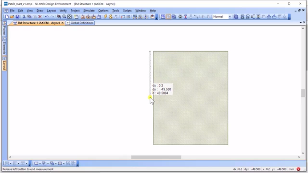
So, let’s center this first. So, this is 100 Y. So, you want to go down to roughly 50, in which is roughly here, and then I’m going to put these down here. And then, I’m going to… there is 50 and this is cool. I am actually holding my left mouse key to keep the measuring there and I’m zooming in with Ctrl and Scroll Bar. So, there is 50, and so I’m going to move this down. That is where I would like to do, zoom back out, Ctrl and middle scroll button and that’s pretty darn good. I might move it up just a little bit. I am perfectly in sync.

Okay, what I want to do is add a port and I go up here and add an edge port and I just click right there and now, I have a port in my antenna. So now, what is going to happen is the EM simulator is going to feed on the energy on the small, little port on that small edge and excite the patch antenna. So, let’s go ahead and set up for a simulation. Let’s go to “Options”, let’s go to “Project Options”, and I want to set the frequency range. I want to set it from – let’s do from 0.7 to 1.2 gigahertz by 0.1 and hit “Apply”. That is not too many frequencies, but I want to get a feel from where it is before I narrow it down. So, I click “Okay” and the other thing is that you can right mouse click and hit “Options”, and I do this to see if it wants me to use and you’d notice “Project Options” that I just set is different from what I set here. So, I’m just going ahead and use “Project Options” and by the way, you can set your “Project Options” in a different schematic. You can set different frequencies.
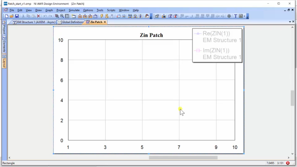
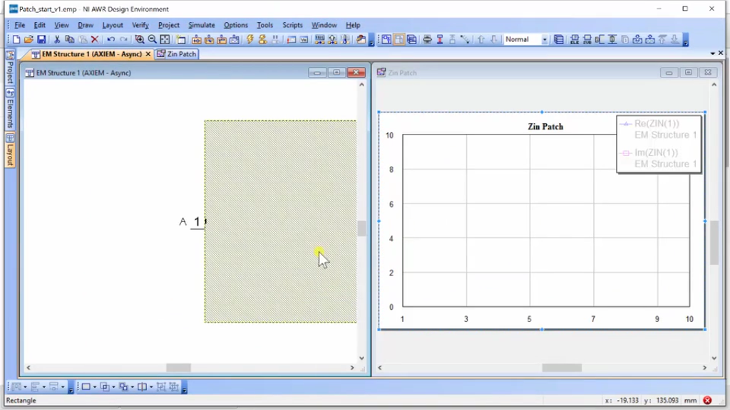
And now, for us to do a simulation, we need to be able to give a measurement. So, let’s go to “Project”, “Add Graph”, and I’m going to call this “ZIN Patch”, it’s rectangular, create, add a new measurement, and here, I’m going to- let’s see where I’ll find this – I think I’ll go to “Linear”… there we go, ZIN. And let’s go ahead and for good, it’s always good to remember to select the source of the data you want to measure. And there is only one port. I could from here select a single frequency, but I’ll go ahead and plot it versus frequency. And I want to plot the real part and I’m going to hit “Apply” and I’m going to click the imaginary and hit “Apply” and now, I have two measurements that are right here. And so, let’s get rid of the Global Definitions, and a nice thing I would like to do is to apply vertically so I can everything that is there.
And now, we are ready to run the simulation. We have our components on the left and we have the measurements on the right and AWR will know exactly what kind of simulator we would like to run. And it’s now – the first thing it is going to do is it’s going to create a mesh and now, it is starting to assimilate. We’ll pause it here and wait until that simulation is done.
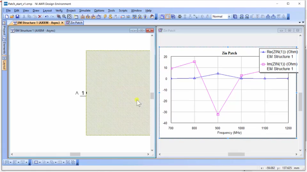
Alright, the simulation has stopped and I just clicked this “Analyze” key to show the waveforms on the plot. Otherwise, they don’t show up. Usually, what happens is that they run the EM simulations, saves the data, and you have to hit the arrow again to run in order for it to do the actual plot. So, what we see here is the real part peaking around 900 and the imaginary part is actually very negative at that value. And that does okay because what we can do is impedance transform this value. Now, if I want to design this antenna, I would actually want to narrow my frequency range. Why don’t we just go ahead and do that? So, I can go to “Options”, “Project Options”, and now, let’s start at 0.85 and we’ll go to 1.501 and we have a few more points, click “Okay”, and now I’m going to re-run the simulation and see if we can narrow down exactly where the resonance is.
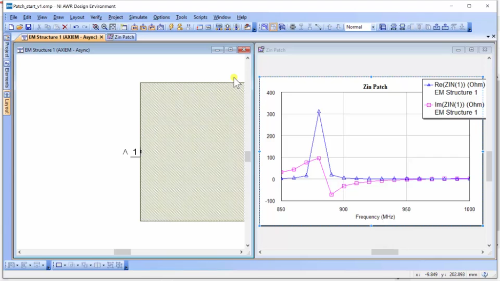
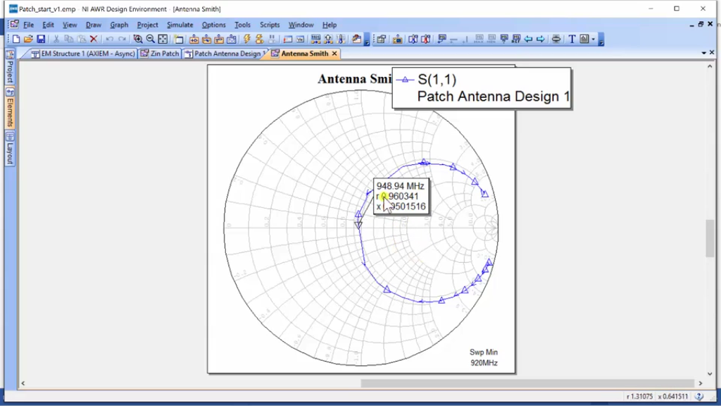
Alright, the simulation has finished and it took about three to four minutes and we can see that we’ve zoomed in. I’m just going to hit Ctrl + M and that is for the Marker. You could just draw – I’m sorry. The menus are context-sensitive and if you look at the top, they change, but when I click it on. So, when I go to graph and marker, add marker, which is just Ctrl + M, I put that there and it shows a resonance of 880 megahertz 311 ohms and that is not too unexpected. The real part tends to be quite high. Also, if you notice the imaginary parts going positive and then going negative, that is actually a good indication of the resonance. And the resonance happens somewhere between the positive and negative transitions. This antenna is tuned right around 880 megahertz. I might run this between 850 and 900 to zero in. Before I did that, I might adjust my dimensions so I could get this peak to 950 ohms. But for the sake of this, why don’t I just go ahead and adjust the patch so that it matches the size that we need.
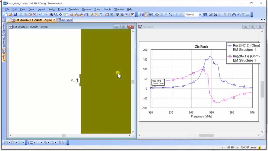
Alright, we’ve run our simulation between 920 and 970 megahertz, with a 0.001; I’ll just make sure that is correct. Yeah, 0.001 and you can see here the ZIN peaks around 950 and it makes the transition from positive to negative right around here. So, this is our resonance frequency. So, we’ve sized it properly and now, what we want to do is create an impedance match network so we can take 50 ohms in impedance matching into this. So, I’m just going to hit Ctrl + M, and go to 950 and there’s my whole marker right there already, sorry. To 950, I’m roughly 166 ohms. Alright, as I have mentioned before, this is an EM structure. So, it’s just basically a copper on a stack-up and what we want to do is to now create a schematic. So, let me go to “Project”, “Schematic”, “New Schematic”, and I’ll call this “Patch Antenna Design 1” and it creates a schematic.
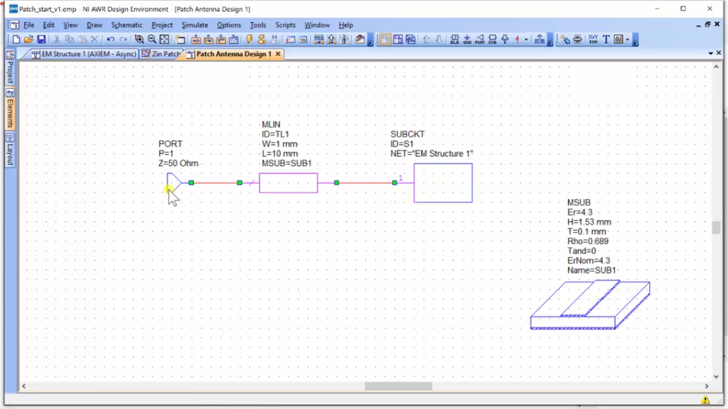
Now, we can go into Elements, Sub-circuits, and we’ll see here that our EM structure is now the component that I can use drag right in there. I have added “MSUB” – by the way, the technique is you hit Ctrl + Land you can just type the word that you want and this is already set up for our simulation scenario and it comes with the file that we started. So now, what I would want to do is I would impedance-match this to 50 ohms and so, what I’m going to do is I’m going to do Ctrl + L, MLIN, which is a micro-strip line in a closed form, put that here, and then I’ll put a port for 50 ohms right over here so you can see this up, okay. Connect these up, done. So, what I am trying to do now is impedance-match my antenna to 50 ohms and I need to figure out what height and width I need to make this transmission line. And if you look at the notes, the calculation is very simple.
And we’re going back for design document and you can see here that the characteristic impedance in that transmission line is the geometrics mean of the two-port impedances. So, one is 50 and the other one, as we saw in our ZIN would be a 166 ohms. So, I’m just going to “Calculator” and I’m going to go 50 times 166 equals 8300 and take its square root; 91ohms is the characteristic impedance of the quarter wavelength impedance transformer. So, I’ve come back to here, but the problem is this is in terms of 90 degrees characteristic impedance, in terms of width and length.
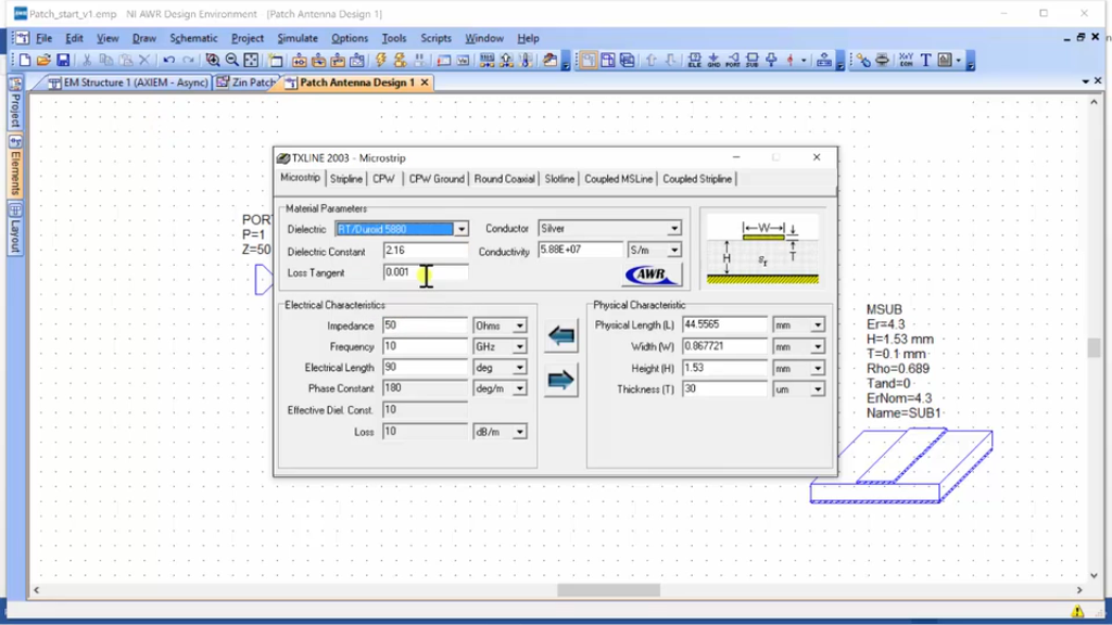
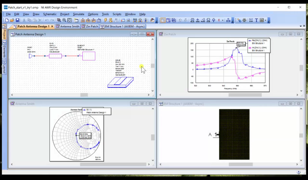
What we do is we go to Tools, TX line, and it brings up a little wizard, and you can select whatever you want here. I selected Duoid, which is sort of a PCV, but let’s see where we would port… alumina. It doesn’t really matter because what we’re going to do is go and change these ourselves to 4.5 with our electric constant, let’s make this 0.005, our conductor is copper, so let’s set everything up front and now, I want this to be 91 on line and I’m going to do it at 950 megahertz and I want the electrical length to be 90 degrees. And if I click the right arrow, it would tell me where the length of the transmission line should be and what the width should be because it already knows the height and the thickness. Now, I believe for half-ounce, this is 18 microns. Let’s just try to get it adjusted so it’s just for a little bit for the thickness of the metal. But, here are our physical length and width. So, 44.7 and I’m going to call that 48. So, 48 and 0.82 millimeters; the length is 48 and the width is 0.8. Now, I’ll run the simulation and for this, I’ll need to create a measurement and so, I could add a graph and this is going to be “Antenna Width” and I’m going to hit “Smith Chart”, right mouse-click to add a measurement, and then I’m going to “Linear”, “Port Parameters”, S11, pop the complex, and this would give me the input impedance of the structure here, including my antenna and my inter-matching transformation and that’s it. Hit “Run”, and you can see that I’m a little bit off here.
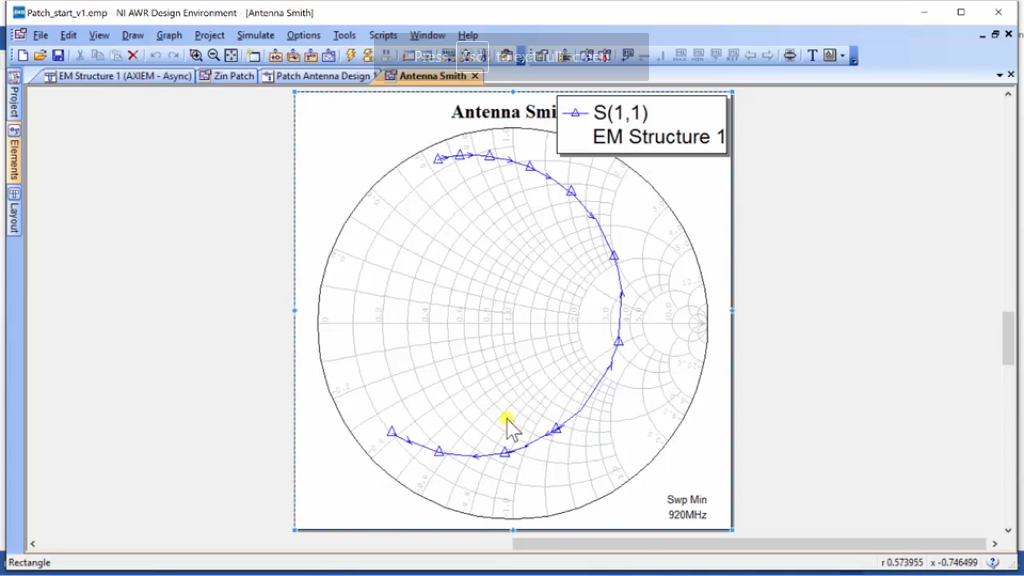
Alright, so the question is why am I off? And if I go up here to the right, I can see why. I just went and added the measurement and didn’t pay attention to the source and this is the EM structure and not the circuit we created. And it’s not the circuit, so what I do is to go back to modify the measurement of the in-structure, and I’m going up to “Source” and select the “Patch Antenna Design 1”, click “Okay”, and then I’m going to place a marker in here. I’ll draw the graph, marker, and I’m going to bring it to 950 and you can see at 950, we’re roughly at 50 ohms.
Now, you notice that it’s giving us a real and an imaginary in decimal format. You can go to “Options”, “Markers”, de-normalize to 50 ohms, and now to give you the actual impedance.
Alright, so we want to take a look at plotting the antenna patterns. And to do this, we need to simulate the EM fields around our antenna at a single frequency. So, what you’re going to do is go to “Projects”, and go to your EM structures, right mouse-click, duplicate; it will create a duplicate down here. We’re going to rename this; I’m going to call this simply as “EM Patterns”, and then you might want to right mouse-click “Options”, and under General, select “Currents”. Under frequencies, unselect using Project Default. We’re going to do a single point at 950 megahertz or at 0.95 gigahertz. Then, you want to go to Axiom, which is our simulator and you want to uncheck “Enable AFS”; okay, great.
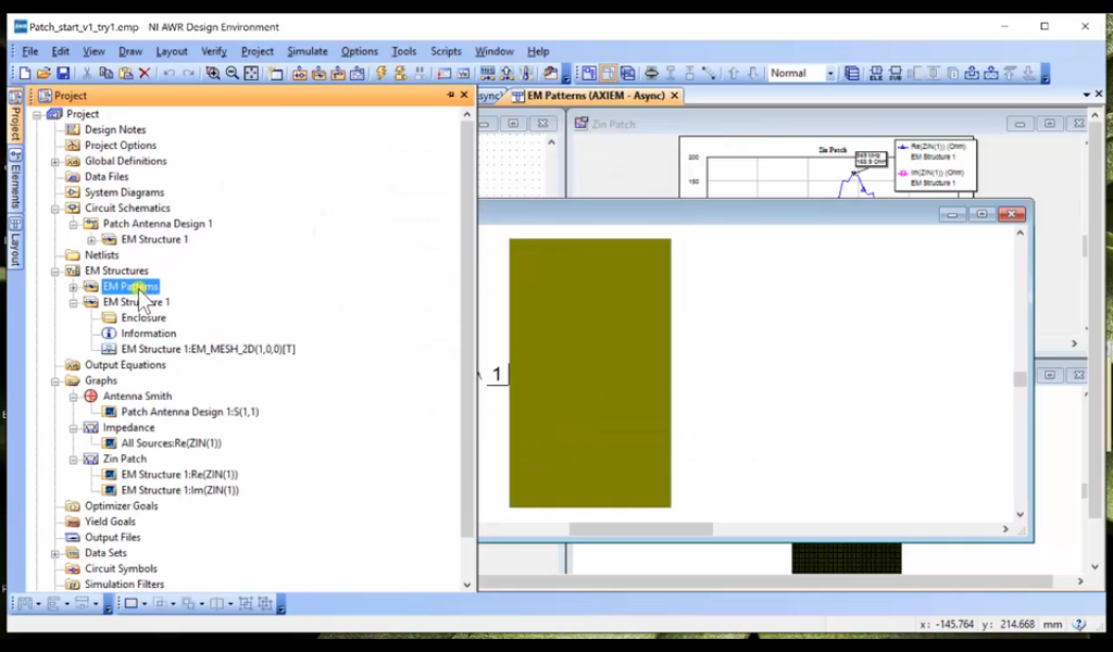
The next thing we want to do is to add annotations so we can see the antenna fields. So, go down to – I picked the wrong one – it’s the “EM Patterns”, “Add Annotations”, select “Antenna 3”, make sure that we’re on “EM Patterns”, let’s plot the total polarization in dB, and let’s do that on 950 megahertz and I’ll click “Okay” here. So, let’s go ahead and run the simulation with now adding this second one. Now, you should note that nothing has changed in the original simulation, so it’s not going to re-run EM Structure 1. It’s just going to run the simulation on this new structure. Okay, let’s run the simulation and all I have to do is to go to my pattern, which is here and I’m going to select “3-D Layout”.
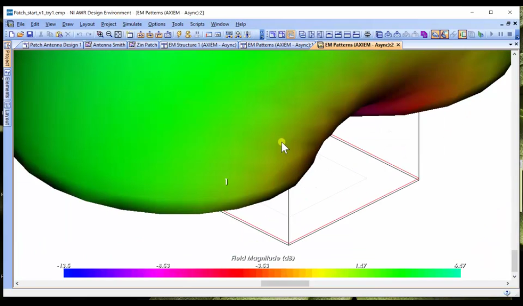
And we can see that the 3-D Layout has been annotated with the field patterns and you can take your mouse and rotate this around. It’s not too difficult and it’s kind of cool. You can see the patch antenna as a very uniform pattern. Near to the center, there is a little bit of a tucking in here and I believe we can – I believe if we were to actually plot the patch, sorry about this, we would see that this gray is the patch and the center is the center of the patch antenna there. So, you can see the field profile and we’re not going to much detail about that, but this is kind of intuitively good to see.
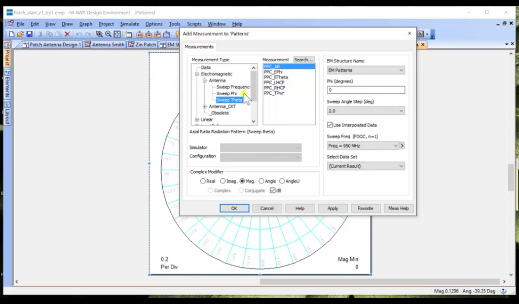
And then, if you want to plot some patterns, and you can go to “Add Graph”, and we want to go down to “Antenna Plot” because we are going to do an antenna plot and we can do “Patterns” and we click “Create” and then we click “Add A New Measurement” and for these under electromagnetic, we find antenna, and we’re going to “Sweep Theta” and I’m just going to hit “Measurement Help” here just to bring up this diagram.
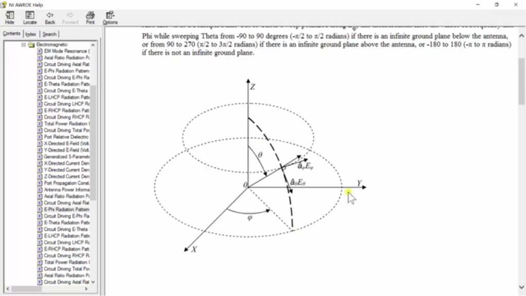
So, what I’m going to do is Sweep Theta and sweep it in the YZ plane and that’s because my antenna is if I can recall if I can see it here, the antenna is a square with the width in the by-direction. So, to get the YZ plane, I just set phi equal to 90, and then I can plot two things. I can plot the electric field in the direction of phi and the electric field of the theta. What is important to note here is that as we specify our point from our measurement by theta and phi, and there are two components of the electric field at that point, b theta and b phi. So, we’ve got two phis and two thetas running around. So, I’m going to sweep theta, hit phi, choose phi to be 90 to get the ZY plane in dB, looks good. And I’m going to do the theta component at 90 once again and 950 dB, hit “Apply”, and now, I’m going to run my simulation and there we go.
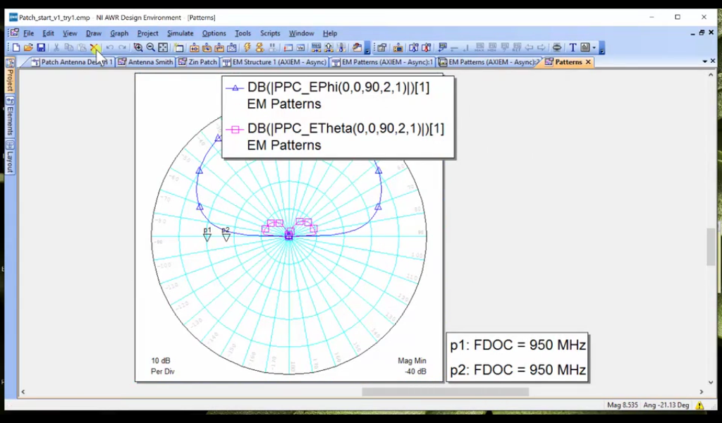
By the way, I reduced the notion at the background so you can see the data is already restored. Here, what we have the pattern of the electric field in phi direction. You can see it has the really nice seeing pattern as we saw at the 3-D plot and the theta component is very small and you can continue on and plot components in the field, the patterns in other directions of fringes. We have Z plane, ZXY plane, but this is a general way on how to get started on both plotting the 3-D and the 2-D patterns.