LNA Design Part 1
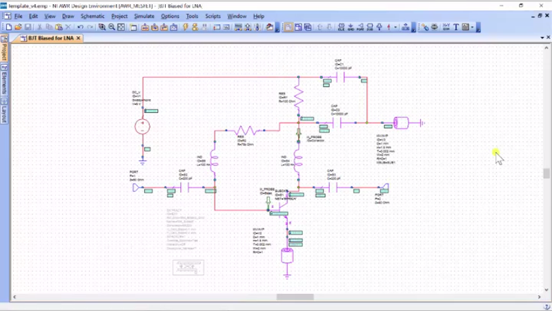
This tutorial is on designing a little noise amplifier. So, you should open up your template, and under your “Projects”, you should see two different bias transistors. We’re going to use the bias for LNA and you can check out the video on BJT biasing to understand how the biasing works. What I would like to do is start off with designing this amplifier and the basic one is done, but what we want to do is pick a load and source impedance that contains two major goals. The first one is high gain, and the second one is low noise and we’ll talk about how we achieve each of those in turn.
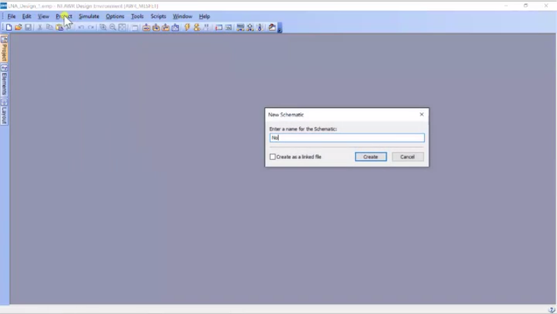
So, let me create – I mean, go ahead and save this project and save it as “LNA Design 1”… okay, great. Now, what I would want to do is to create a schematic, show the project as “schematic” and I like to call it “Non-linear LNA 1”. The reason why I use the word “non-linear” is we’re using a splice model in this simulation as opposed to the S-Parameter model, although, AWR can calculate the effectiveness of the parameters from our non-linear splice model.
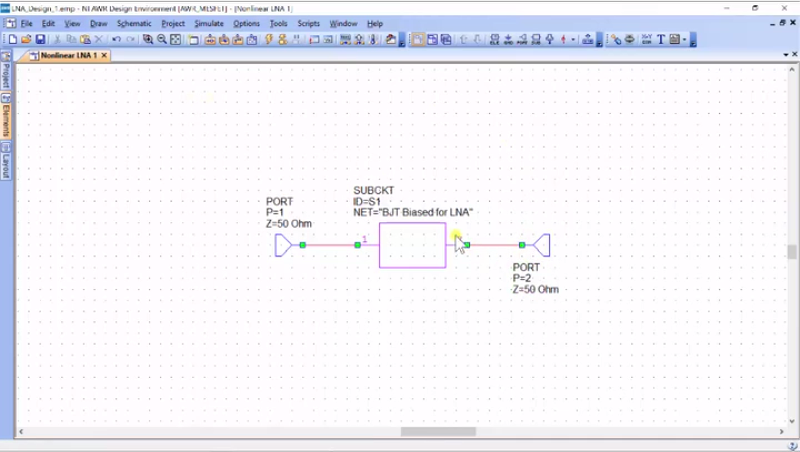
So, we’re going to create and you just have to go into “elements”, into “sub-circuits”, and you will see right there. That we have BJT bias for the LNA and I’m just going to pop that into right there. So, let’s just go ahead and do something real similar. Let’s just see what its gain is. Now, the two metrics I would like to use is that let’s add a graph, and we can do “Smith”; this is good for seeing…
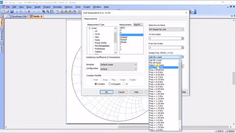
Alright, let’s set up some linear measurements and we’re going to add to the graph a Smith Chart, and click “Smith”, create, and now we want to add a new measurement, “S11”. Make sure that you get the right device, make sure that you use the X-axis for our frequency. By the way, you can select individual frequencies or even use the tuneable, but we want to use frequency for that, apply, let’s do S22, apply… great. And then, what we want to do is add a graph and I’ll call it “Linear Performance” and we’re going to get a rectangular here. And initially, I’m just going to add on “S21”. Okay, everything is set there and we will do that in dB and I’m just going to run.
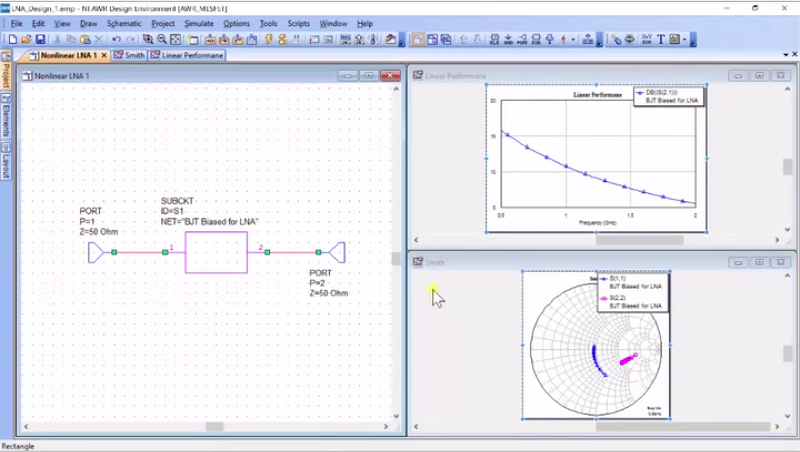
Alright, so if you go click the schematic and do tile vertical, we’re going to split everything up. So, these are looking at my input impedances and this is looking at my gain. And let’s just go ahead and put a marker on here, get a graph marker and I’ll make this big.
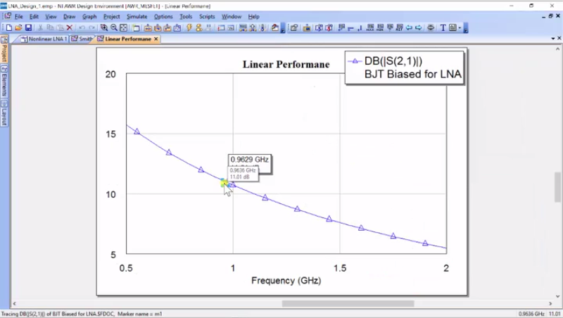
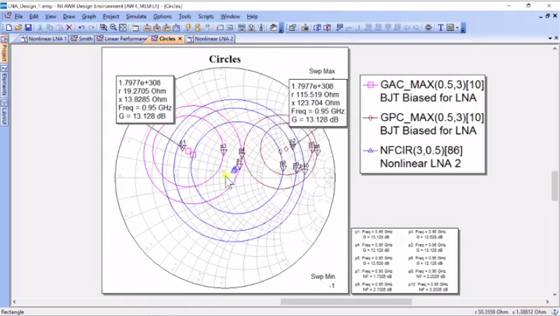
So, we’ve got… It’s not so bad. We’ve got 11dB of gain at 50 ohms at the output, which is not too bad. In fact, we’ll find out that we’re getting a lot better once we implement everything, but what we’ve done now is we have a small signal simulation. So, if I descend into here, we have a transistor on this non-linear. What AWR has done is it has calculated a device point and then figured out the AC equivalent circuit and then because we have asked it to do a Smith and as to one measurement, it just says, “I just need a small signal” and so, we’ll do a small signal measurement around that bias point to give you these values. Now, one thing I would like to caution you on – we’ll follow this back up here – and to make this a little more fun for us, I’m going to change this to a BJT and we’re just going to amplify it… there you go. Now, what we can do is find out if there is a source of load impedance that would actually improve our gain. And AWR has already been calculated the S-Parameters of this block and using the Microwave theory, there are several equations in particular for something called G-Max, where we can calculate the maximum possible gain and we can also calculate the source and load impedance that will give that to us. And an easy way to do that is to use what we call the gain circles and so, let’s plot those; they’re pretty easy. So, “Add Graph” and we’re going to go to “Gain Circles” – Actually, I’m just going to call it “Circles” and we’re going to the Smith Chart. And I’m going to hit “Create”.
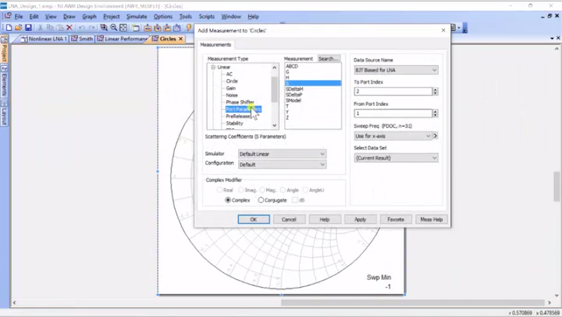
And now, what I’m going to do is I’m going to add a new measurement and we’re going to go to “Linear” and I’m going to “Gain” here, and I’m sorry, I’m going to “Circles”; gain would give me a single value. What “Circles” are going to do is they’re going to show a range of impedances that give you the same effective gain and if you have studied Microwave Theory, you will learn that for a system of input and output impedances, there is a constant gain on a circle in the impedance plane and so, when you map with the bi-linear transform, you will find that constant gain maps to circles in the impedance plane. We’re not getting into that, but this is where the system is coming from. So, the first thing I’m going to do is plot the available gain circles using G-Max and I’m going to do a – let’s just do one for now. So, this is going to plot the maximum point. So, I’m going to hit “Apply”, and let’s actually calculate this just for one frequency; otherwise, it’s going to calculate them for all the frequencies and obviously, you can’t have different impedances for every frequency for our basic BSL. We’re going to change that and then the other thing we’ll add is power-gain circles using G-Max. And once again, I’m going to select a few megahertz…
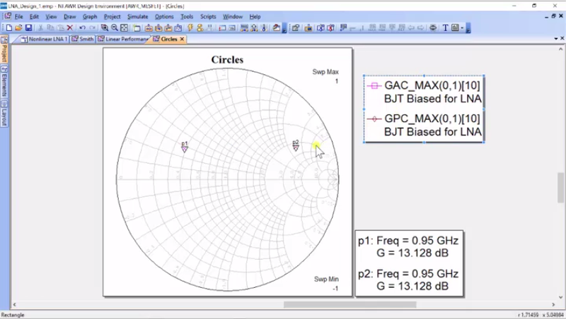
And I’ve added this one that I don’t want. So, the way that I get rid of one is to go to this and I will delete it and it’ll say “yes” and there we go. And then, I will simply run this. Okay, so what has it done is that it’s given me the AC-Max and the GP-Max, you wouldn’t notice from the description, but this GP-Max over here is actually the optimal load impedance for G-Max and maximum gain and then, this is the optimal source impedance for gain. So, pink here is going to be a source and brown is going to be the loop. How do I know that? You have to search through some of the documentations and understand how everything is derived. For now, you can just use this as a given. And what you would notice down here is that the gain is 13.127 dB at these two points and that is a couple more dB than we do have. And what’s nice about just putting one point in our plot is that we get this easy and so, we can go back and modify our measurements and I’m going to do three circles and make them 1 dB each and this is the available gain.
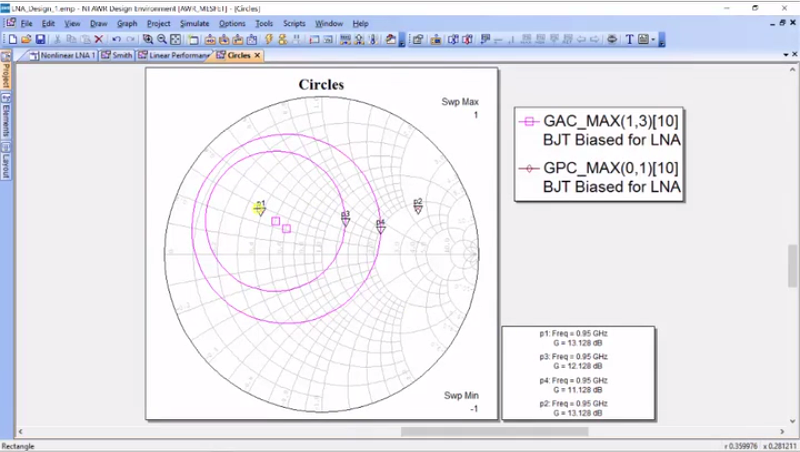
And so, you can see that what it did is that it added circles around the center-point. And what the means is – so, P1 here is for 13 dB and this is a 12 dB circle and any input impedance along this circle would give you 12. That is why circle is at constant gain and in fact, if you had any impedance inside this circle, it would give you something between maximum gain and we have another circle here and let’s just go ahead and modify the output. In GPA, we do the same thing and we’re going to do 3, and I’m going to do these in 0.5 dB in steps; there we go. In fact, I’ll go back and modify this one to get this 0.5 dB in steps. So now, here are the impedances for the input, and here are the impedances for the output. Let’s just add a marker because that will help us know what the impedances are. And this is all normalized to 50 ohms. So, you can go to “Options”, you click on “Markers”, de-normalize, it’s already set to real/imaginary impedance, click “Okay”, and now we can see the source impedance that gives us the maximum gain. Now, what I want to do is to do another marker… there we go, and you can see that it gives us the maximum load impedance per gain. Now, I just want to do a quick trick here. So, I want to come into the next non-linear LNA 1 and I’m just going to duplicate it and I’m going to call this “2”.
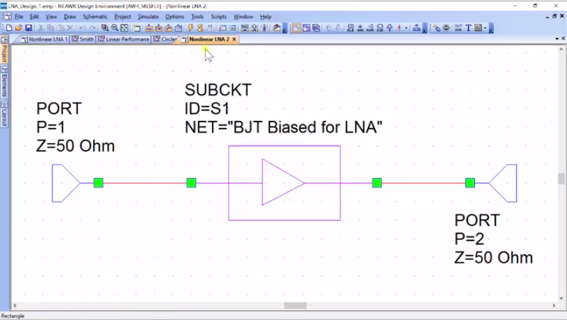
So now in here, it’s the non-linear LNA 2. So, here’s the trick you can do. You can actually change the port impedances, which is the equivalent to applying the impedance to the input here. And so, what I’m going to do is to say, “Okay, it’s 19.2 plus 13.8j.”
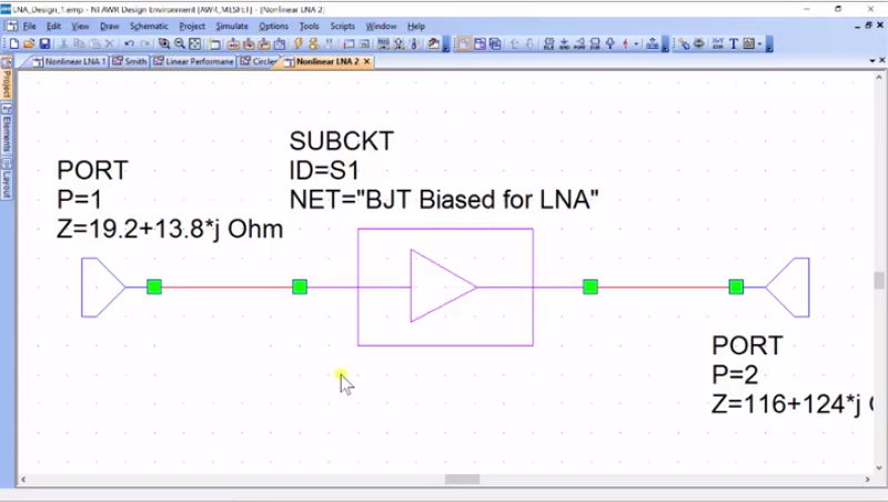
“19.2 + 13.8*j”… Okay, it’s kind of interesting that I just popped it as my impedance and if I go back over here, this is where we call it “116 + 124”… “116 + 124*j”. We’ve set these impedances and now, what I want to do is to take a look at the actual gain. So, I’m going to the linear performance and I’m going to add a new measurement. Here, I have to select my non-linear LNA 2, and then I’m going to do port parameters S21, use the X-Axis, but in dB… okay. And then, let’s go ahead and run the simulation.
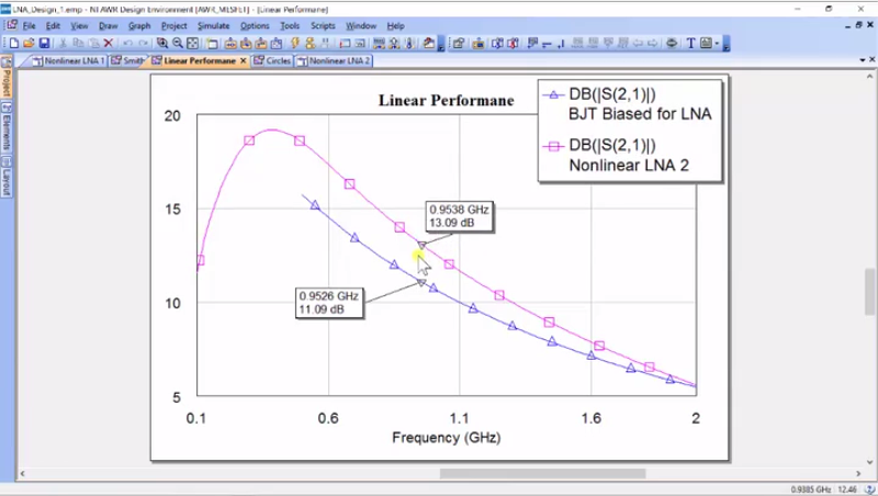
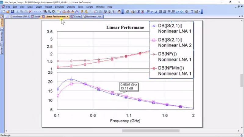
Alright, so what do we see here? Well, we see that we have a higher gain, and let’s take a look on what that is. So, at 0.950 GHz, let’s see if I can get to 0.950 as it should come out exact. Okay, 13.11 dB of gain and if you’ll notice, we did our gain circles; it told us the maximum gain we could achieve is 13.128. So, this is pretty simple. This is just like in impedance matching in linear systems, and we do the same thing to maximize our gain for the transistor. We use the Microwave theory to calculate the circles and then these circles tell us where the impedances are and what’s nice is the source impedance or the load impedance actually could be anywhere near here and we would only drop by half a dB of gain. So, this is the first step in designing the maximum gain. However, for low-noise amplifier, we’re also concerned about the noise and getting into noise theory, both on what is noise and how it affects amplifiers is outside the scope of this workshop. However, I would like to go over just briefly over some concepts of noise to understand why and how we can tune for noise.
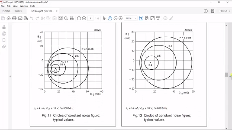
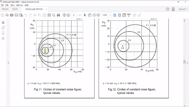
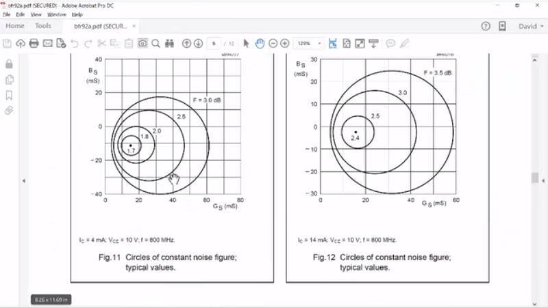
So, I’ve pulled up here the data sheet for the BFR92A, and I’m just going to scroll down. This will be online, so you can take a look at all of the aspects and I want to show you a couple of things. First off is this. So, these are “Circles of Constant Noise Figure”. Just like we had impedances that would give us maximum gain, we have impedance circles that would give us noise figure. So, the lowest noise figure, which is our target, and in this example, biased at 4 milliamps – this is at 800 megahertz – is right here. So, this is a GS and a BS and you have to convert that to your resistance impedance, but 1.7 is the minimum noise figure for this. And in this case, it is 2.4 and you can see it’s mapped out on this chart and I just want to say, “So, this is the first part.” If you want to understand why the impedances affect these, let’s just take a quick look at a document that I’ve pulled up that is in our noise circles.
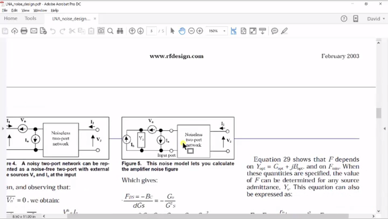
Alright, let’s just take a quick look at how impedances would actually affect noise and I’ve placed this article up there. It will give you a brief introduction, but I just want to scroll down and show you one picture that will hopefully give you a little insight into this. So, when we model a 2-point network, such as an amplifier, one of the things we can do is we can remove all of the noise in the amplifier and model it with two sources at the input. Now, there’s a voltage source for the noise, and a current source for noise and this would be ideal and this could simply be a transistor or a passive network, although passive network would have a very simple noise. Now, why do we have both the voltage and a current noise model? And these immediately seems a little confusing, but let me just explain the following.
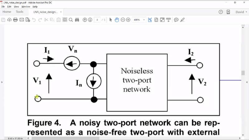
If I had to short the input, so I had to make the source input zero, then what would happen? This current source would just circulate through that short, and none of the noise current would ever get into our network. However, if I short this, then the voltage noise is 100% going into our network here because this voltage would then be – this would be ground, and this would be the positive node and so, all of our voltage node goes in. And so by shortening, we basically cancel out the current noise, but we all have our voltage noise. Let’s take the opposite where I just shown here. So, this is open. If this is open, then no current can flow into the voltage node and therefore, none of the noise from this noise source can enter our network. However, the current noise can enter the network through its input impedance and so; we would get all of our current noise here. In reality, we have something between a short and open in our input. Therefore, we have partway of this voltage noise and partly of this current noise that affect. And once again, these are models that we have calculated the noise network and extracted out what would be the effective voltage and the effective current noise of the device and we need both voltage and current because we don’t know what source impedance we’re going to meet. Now, that is how we model noise in transistors or amplifiers and it turns out that…
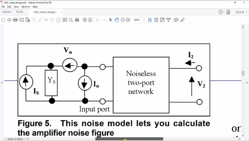
If you apply an impedance here between zero and infinity, the actual noise that enters the network changes and depending upon the exact relationship for the voltage noise and the correlation between the voltage and current noise, which typically there are because they both relate to the same device, there would be an impedance here that minimizes the noise of the system.
And that impedance is what we see in our previous slide of the constant noise simulations, so the optimal impedance, which minimizes the noise, is the one right at this point and it provides a noise figure 1.7 and then, there are circles of impedances that provide higher and higher noise. So, this impedance at the source is just trying to basically manage these two noise sources and trying to minimize their effect on the network.
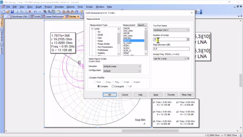
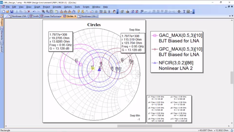
Okay, so if you might think this is a little bit crazy, let’s take a look at it from our device. And now what I’m going to do is to add a new measurement; I’m going to noise… noise figure – I’m sorry; I mean circles, noise figure circles, and we’ll do a number of circles as 3.5 dB there, click “okay”, and then we’re going to run and this looks pretty ugly. We’ve forgot to select the single frequency. Let’s go back and select a single frequency of 950 megahertz… there we are.
Alright, so the blue is the optimal noise, the pink is the optimal gain, and these are both from the source and we went through Microwave theory to find out that the noise is not affected by the output of the amplifier, but only the input impedance of the amplifier. So, we’re only looking at the input. So, let me just add a marker and so if I add this marker here, we see that the noise figure at the center would be 3.2 with this impedance and 950. And so, in designing an LNA, what we are trying to decide is first-off, we generally try to get load impedance that maximizes gain. So, we try to pick this point 2, our 115 + 120 x, but when we want to pick source impedance, we have to choose between maximum gain and minimum noise. And typically, what we want to do is find a compromise. I know that if I moved to this circle here, I’m simply in the half a dB below in gain. And this circle here is 1dB; let’s actually go in there and modify our noise figure measurement so that – okay, it is a half a dB. Let’s do 2.2 for our noise figure… there we go.
As you can see even at this point, we’re less than 0.2 dB away. So, I’m going to choose this point as my source load and I did it based upon a judgement call between gain and noise. And so, the source impedance that I’m going to design for is 45 + 15 and the load I’m going to design for is 115 + 123. Now, what I would do is to go over to the video on synthesizing impedances using the I-filter matching tool. And then, I’ll come back and insert those into my design and simulate again. So, let’s take these impedances and put them back into our original circuit, the non-linear LNA 1. So, we want our source to be 45 + 15.6j.
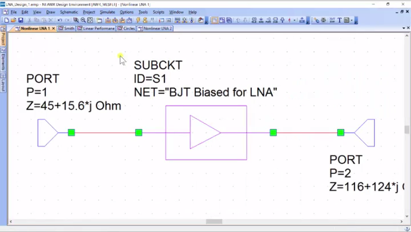
…45 + 16.4*j and I’ll just go back and check that, if I had that wrong. 45 + 15.6, yeah… 15.6; there we go. And then, the load is 116 + 124; I’m going to approximate… 116 + 124*j and once again, I’m just going to check that… yeah 124, great. Alright, so I’ve done this and so let me go to my linear performance. So, this was with optimal impedance. So, this is with 50 ohms. Now, we change our impedances and so, what we’re going to do is to get the impedance for our new impedances. So, let’s just go ahead and run that. And so, this is LNA 1, we’ve got this here, and so, I’m going to go to my linear performance and I’m just going to modify this measurement of… I really want non-linear LNA 1… okay, there we go.
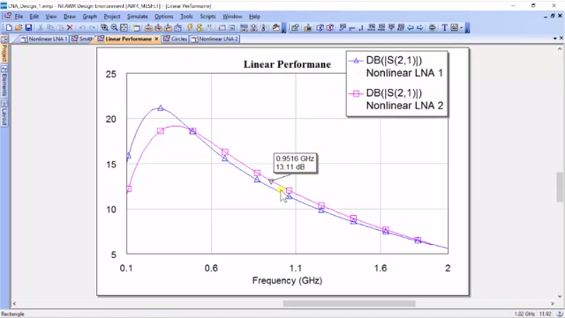
Okay, before I was measuring BJT, but it is very similar and so what we see is that we’re almost the same in gain and that is what we would expect because the circle we have chosen is almost near our optimal impedance, but let’s go ahead and add something.

So, let’s go add a new measurement, and now one thing we can add is noise and we can add noise figure and I want to do this for LNA 1, and hit “apply” and noise figure minimum, “apply”, and then I’ll show you a trick. You can go to “Options”, “Measurements”, “Auto-Stack”, and it puts everything together. And actually, we’re going to put some of these things together. If you go to “Measurements”, you see that we’ve got – here are 2 S21’s. We will put these both on the bottom. We’ll put the two noise figures on two, and then you can just go to – I’ll just pull back – we added the fourth when we hit “Auto-Stack”… okay, great. So, what we see here is at 950 megahertz, we’ve almost have the same gain and our minimum noise figure is the red. So, this is basically if you had the absolute ideal source load. Here’s the minimum noise figure you can get from frequency and you can see 950 megahertz were pretty darn close. So, this is a pretty good design. Now, I want to talk just a moment about this idea of minimum noise figure because let’s just go back to our data sheet.
And you’ll notice that these noise circles were particularly biased and we can see that at a higher current bias, our minimum noise figure is much higher. And so, the minimum noise figure tracks in some fashion with the bias current, and the data sheets generally tell us this.
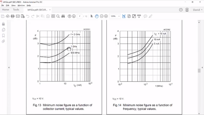
And in fact, if we scroll down, you can see the minimum noise figure as a function of a collector current. So, in one gigahertz, our minimum noise figure is just below 2 and that occurs at one or two, probably between two or three milliamps whereas we’re operating around 5.
And so, we’re going to be up here as our noise figure. Let’s just go back to our schematic here and you can see that we’re a little bit below to our noise figure to bias in. So, not only we want to design impedance to give us the optimal, we also want to design the bias current to give us the minimum noise.
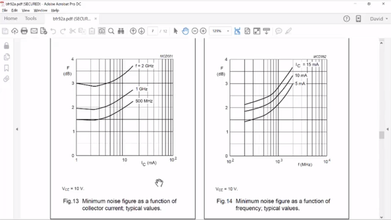
And as you can see in this configuration, it suggests that the noise figure around 1 gigahertz would be a little less than 2 or the sum between 1 and 500. So, we should be right in here and that’s where roughly what we solved for our noise figure to be around – let’s just put a marker on it – okay, 1.7… Let’s go to 950… there we go, 1.778 and if you go here and look at the data sheet, that’s going to be somewhere around here. So, this is very consistent with what we have. Alright, so that is really the design. The next thing is simply to go to use the I-filter wizard to create an impedance synthesis so we can terminate our source and our load with the correct impedances at our RF frequencies.