BJT Biasing

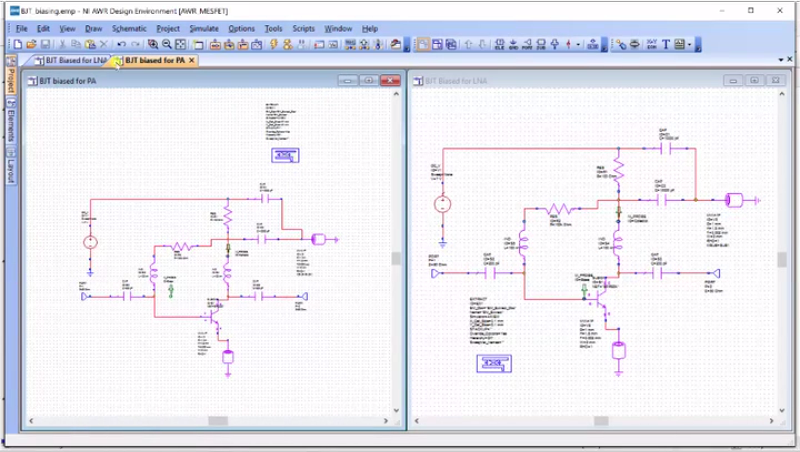
So in this tutorial, we’re going to take a look at the Bias for the BJT transistors. And I’m going to save this project as “BJT Bias”, and overwrite that. Alright, so in your circuit, you will see two schematics, BJT Bias for the NA and BJT Bias for the PA. And for the sake of this tutorial, we’re just going to disable the extractions.
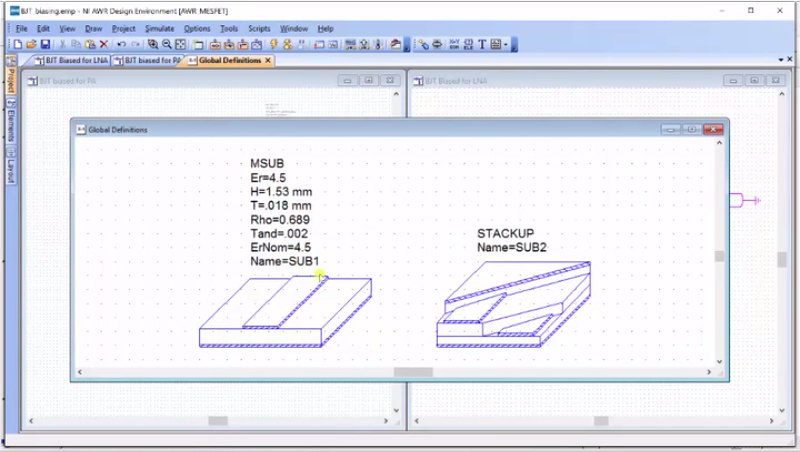
Now, I should point out that in our projects in our global definitions, we have the substrate description and also the STACKUP for EM. So, we don’t see these explicitly on schematics, but they are in our global definitions.
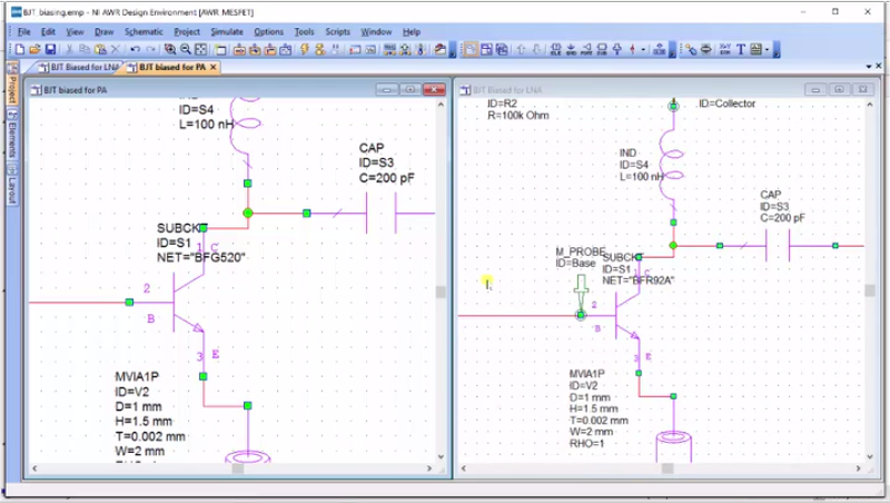
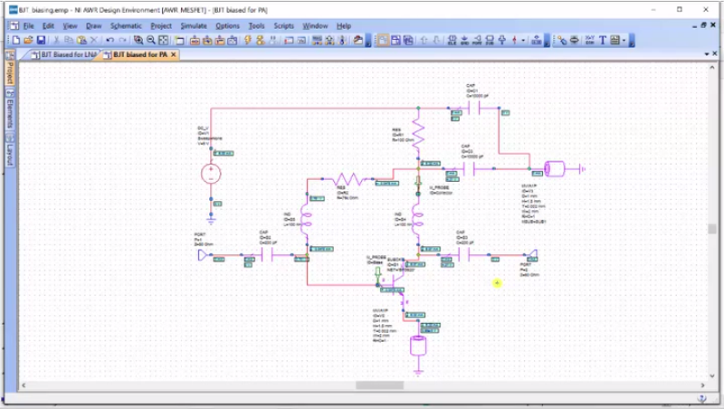
Alright, so let’s go take a look at these, and what you should see is that they look very much the same. In fact, if you went through, I think you’d find them almost identical, but the only real difference is this has a BFG 520 and this has a BFR92 Transistor. But, let’s just zoom out a little bit and take a look at the schematics and we’ll see that they have exactly the same Biasing structure. And that makes sense because they ‘re Bipolar Transistors, and so the base emitter junction can mean roughly the same and it turns out that the beta is roughly the same and biasing them is almost identical and it makes sense. So, I’m just going to pick one of them. We’ll take the LNA here and we’ll look a little bit closer at the schematic. Alright, it’s close enough one more time…
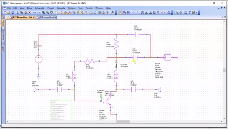
Alright, so what you’ll notice is we’ve got our bipolar transistor and it is grounded through this via. And so, this via is just simply a part of the layout that’s there. I’m just going to adjust this to make it a little bit nicer. So, this is ground, this is the common emitter, and we want to bias this to split into a certain base kind because of the number of bipolar transistors is on current-based devices as opposed to the loss that is voltage-based. The way we’re going to settle the DC bias current, is through a resistor and this resistor here is set for a 100K; I found out that 75K is a little bit better. But, the current that flows through this node – notice that this inductor will be short at DC and this capacitor will be open – is simply the voltage here at M-Probe called Collector, the voltage of this node, minus 1VBE, above 0.7 volts, divided by the resistor and that’s going to set the base current. Now, the collector current is going to be the base current times beta and let’s look at the output. We’ve got a DC choke. So in DC, this is a short, but in AC, it’s going to be an open. Likewise, the capacitor is open at DC and it will be short at AC. And so, all of our DC current will flow through here and one part of this biasing that you may not have seen before is the fact that we have our collector current flowing through the resistor to this node and this node is used for the bias. And this is just a little bit of collector bias feedback and you can understand how it works by imagining that beta, instead of being 100, was 500, just as an example. Then, for given base current, we have a lot more collector current. That collector current would create a large IO drop at this resistor, this voltage would fall, and as the voltage fell, there would be less current flowing into the base and the collector current would reduce and it would find a stable operating point. So, this resistor here is just a way to set a feedback because the collector current determines the voltage on this node, the voltage determines the base current, the base current controls the collector, and so, there is a nice, little feedback loop here which works out really well for bias and transistor. You could, in our design, just take this resistor and put it to the supply and it would be okay. We have in our left our supply voltage and typically, we’re going to have to choose 5 volts in our designs, and then we have two decoupling capacitors. So, one decoupling capacitor on the supply, and another decoupling capacitor right here on the top of this inductor. I was like to have a very short circuit path for any RF current that would have for high frequencies. And so, this is already set to be biased and all you have to do is you could run a simulation, but let’s just go ahead and do something here.
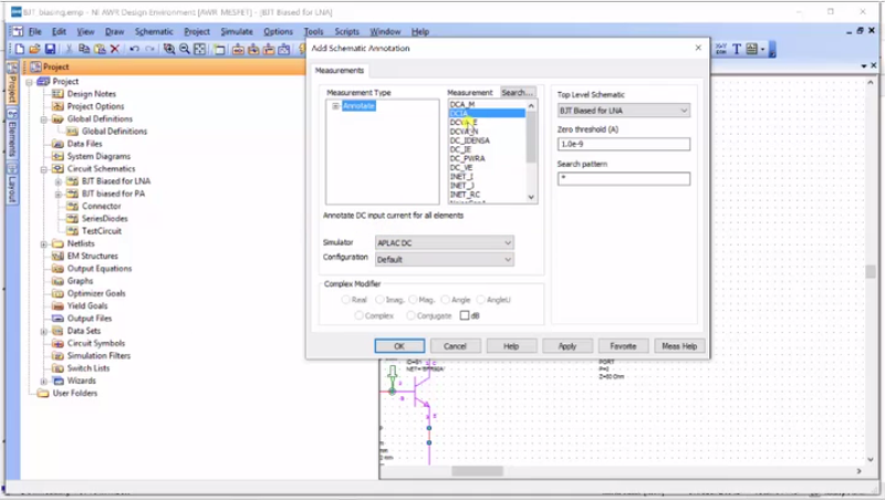
Let us go to this schematic for the LNA and I’m going to direct my mouse to click and add an annotation and here, I can add DC input currents for all elements. I’m going to add that and then I’m also going to do the DC voltages for all nodes, and then I hit “apply”, and if you go in here, you could see we had this already set up, but then, what I’m going to do is hit “run” and it’s going to run a DC analysis point and gives us our current. Let’s just take a look and see what we’ve got here. I’m just going to zoom in. By the way, you could just zoom in by hitting ctrl and scrolling your mouse-wheel.
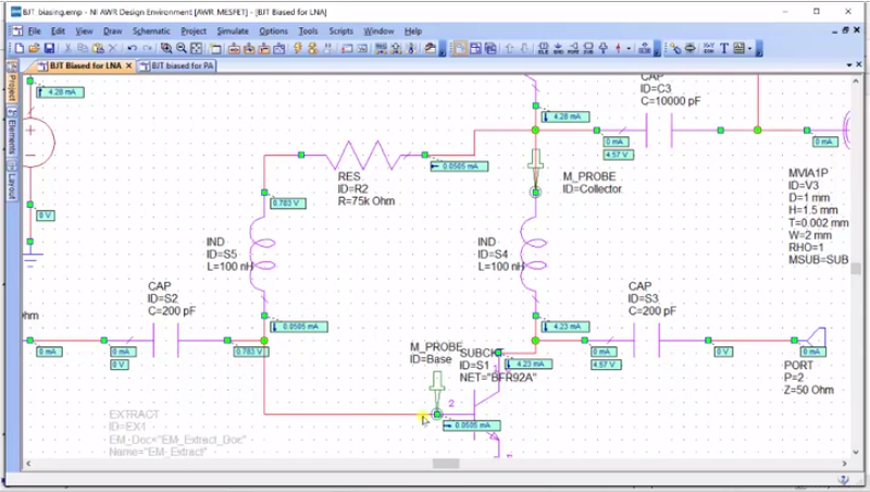
So, I have roughly 50 microamps flowing into the base and I have roughly 4.2 milliamps as my collector current and we can see here that this voltage in this capacitor is 4.357 volts, which is a little bit below the 5 volts that we have here. So, you can see where the collector current has pulled this down to create a lower voltage and also a feedback loop. I could just go here and I could just do 60K and I could rerun that and I could adjust my current going on through here and you can see that DC-wise, the inductor is indeed a short. And here we are now at 5.2 milliamps. So, I could go to this circuit and design a different-based resistor here to bias it up.
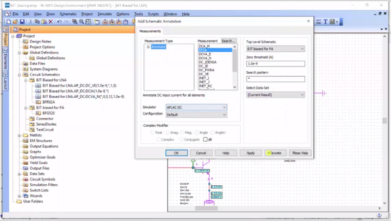
Likewise, I could go to my BJT that’s biased for the BFG 120 and I could just go to “Projects”, right mouse-click, annotate, and I could do the currents for all elements, apply and I could do no voltages, apply, and there we go, and I’ll run this.
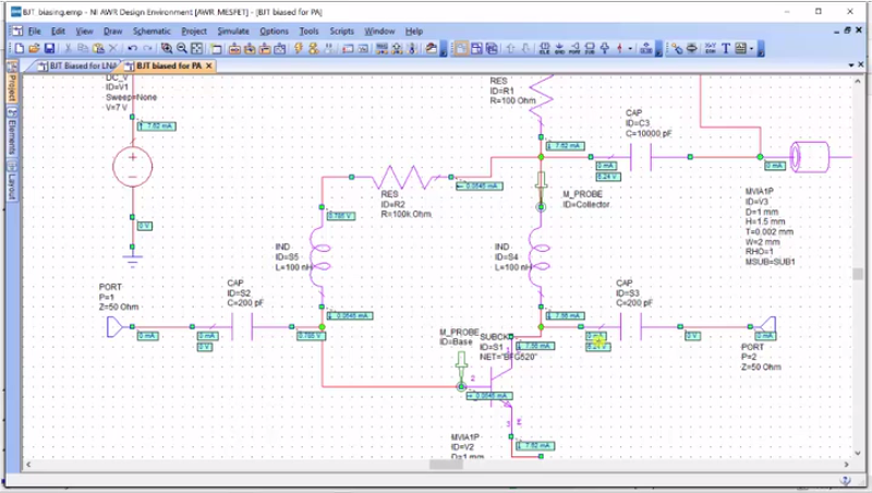
And here we are for the PA and what you’ll notice – let’s just set this back down to 5 and rerun it, and there we go. We’re running about 5 milliamps in bias current for the PA and we could have adjusted that by – I’ll bring this here. And one thing you will notice is that the BFG 520 has a little bit higher beta, little bit higher gain, and it’s also a higher frequency transistor, which helps out for our PA.
So, this is how we set up the bias and the way you are going to operate with this is that you basically going to send a RF signal on the left, and you are going to get an RF signal to the right and that is what we are going to use for our RF path.
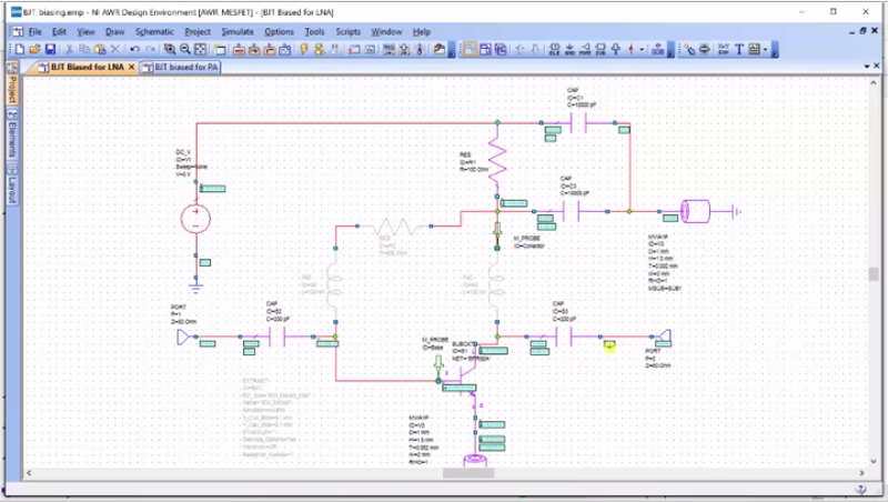
And just to be clear, – we’ll go back to LNA for this – when we have our RF flowing through, this is the path; it flows through here and out of these two capacitors. Everything I just made grey is part of the DC biasing and it would not be seen by the RF path. So, what is important when you are doing layout, and by the way, we could go look at the layout, which is already down by clicking “View Layout”…
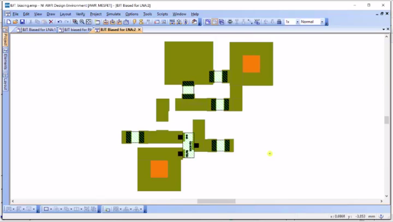
And you will notice these parts have disappeared because I disabled them, so I will just put them back… there we go.
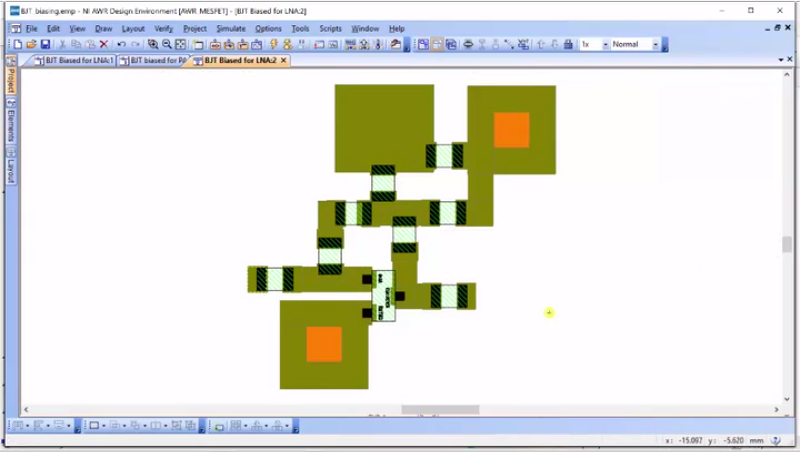
And you can see this is the RF path that comes into the base after the collector and this is really what you have to watch out for your layout. This is the DC biasing and this is the vias, and this is the supply path where you would bias up your supply voltage. Likewise for the PA, you could look at its layout, and you’d notice that it’s very similar, not as much as care is taken in the layout, but it functionally works very well. Alright, so this is basic how we bias up our BJT transistors for our amplifiers.